P R E L I M I N A R Y | AMD |
|
|
The SRAM is intended to serve as a shared memory re- source between the driver operating through the system interface and the 80188 core operating through the Am79C930 memory interface bus. Even though SRAM memory locations 0 0400h through 0 043Fh are acces- sible from the system interface, these locations cannot be used for
PCMCIA Attribute Memory Resources — The PCMCIA standard requires that each PCMCIA device contain a Card Information Structure (CIS). The CIS contains information that is used to provide possible configuration options to the system.
The PCMCIA standard requires that the first tuple of the CIS should be located at Attribute memory byte 0h. 1K of Flash memory space is mapped into the lowest 2K of PCMCIA attribute memory space to accommodate this requirement. Since odd addressed bytes of Attribute memory are undefined, these addresses are not mapped to the Flash memory. The 1K of Flash memory space that is mapped to Attribute memory space is also
visible as common memory. The upper 32 bytes of the 2K of attribute memory space must not be used for PCMCIA CIS information, since these bytes map to the upper 16 bytes of the Flash memory, which will be used by the 80188 core of the Am79C930 as the initial instruc- tion locations after reset.
Note that the Configuration Tuple must contain the value 800h for the TPCC_RADR field, since the Card Configuration Registers within the Am79C930 device are located at this fixed offset.
The PCMCIA Card Configuration registers that are sup- ported are the Configuration Option Register and the Card Configuration and Status Register. These two reg- isters are physically located in the Bus Interface Unit and logically exist only in PCMCIA Attribute Memory space. They are located at Attribute Memory locations 0800h and 0802h, respectively. The location of these registers is fixed. Therefore, the information pro- grammed into the CIS must give the value 2K (=0800h) as the Card Configuration Registers Base Address in the TPCC_RADR field of the Configuration Tuple.
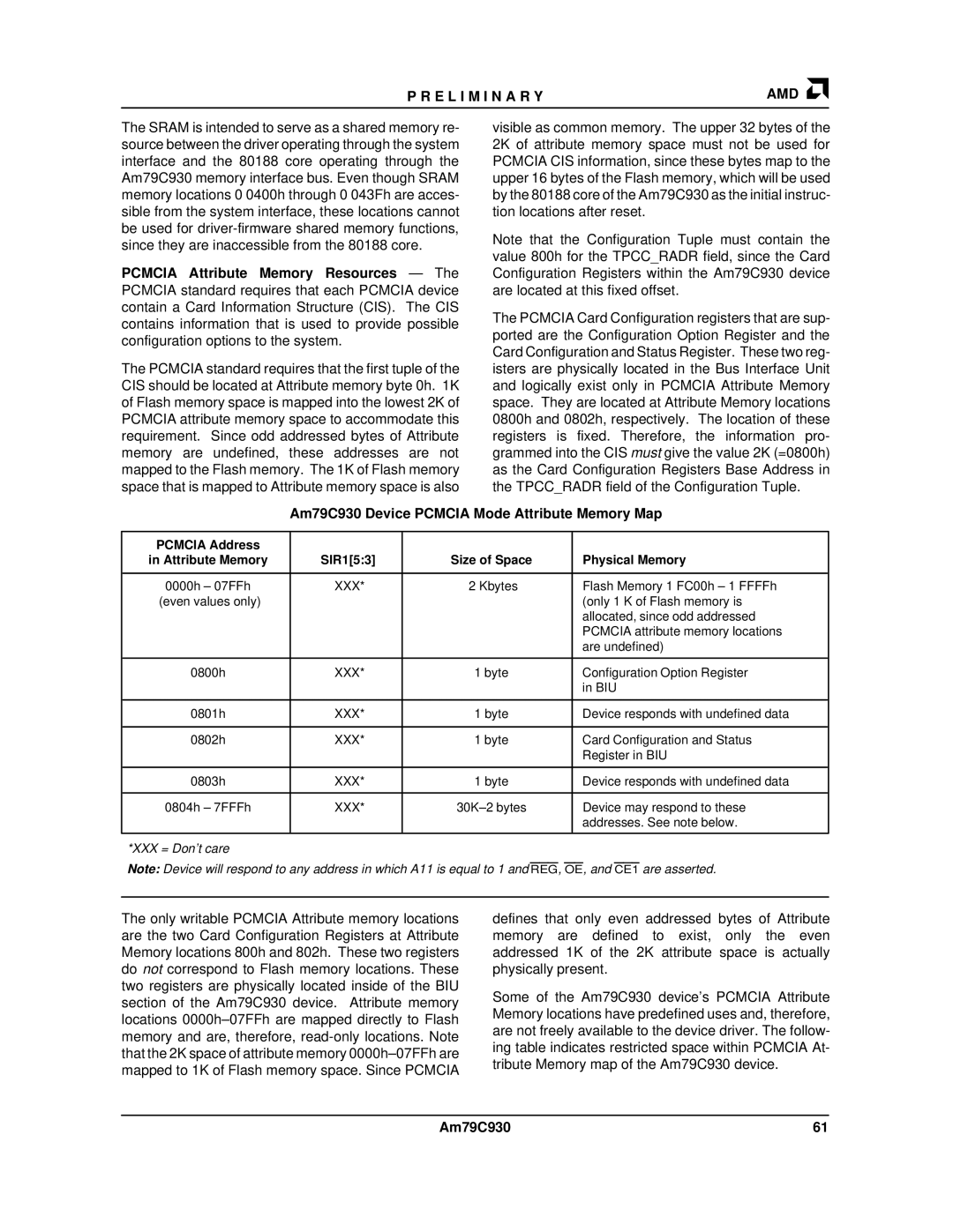
Am79C930 Device PCMCIA Mode Attribute Memory Map
PCMCIA Address |
|
|
|
in Attribute Memory | SIR1[5:3] | Size of Space | Physical Memory |
|
|
|
|
0000h – 07FFh | XXX* | 2 Kbytes | Flash Memory 1 FC00h – 1 FFFFh |
(even values only) |
|
| (only 1 K of Flash memory is |
|
|
| allocated, since odd addressed |
|
|
| PCMCIA attribute memory locations |
|
|
| are undefined) |
|
|
|
|
0800h | XXX* | 1 byte | Configuration Option Register |
|
|
| in BIU |
|
|
|
|
0801h | XXX* | 1 byte | Device responds with undefined data |
|
|
|
|
0802h | XXX* | 1 byte | Card Configuration and Status |
|
|
| Register in BIU |
|
|
|
|
0803h | XXX* | 1 byte | Device responds with undefined data |
|
|
|
|
0804h – 7FFFh | XXX* | Device may respond to these | |
|
|
| addresses. See note below. |
|
|
|
|
*XXX = Don't care
Note: Device will respond to any address in which A11 is equal to 1 and REG, OE, and CE1 are asserted.
The only writable PCMCIA Attribute memory locations are the two Card Configuration Registers at Attribute Memory locations 800h and 802h. These two registers do not correspond to Flash memory locations. These two registers are physically located inside of the BIU section of the Am79C930 device. Attribute memory locations
defines that only even addressed bytes of Attribute memory are defined to exist, only the even addressed 1K of the 2K attribute space is actually physically present.
Some of the Am79C930 device's PCMCIA Attribute Memory locations have predefined uses and, therefore, are not freely available to the device driver. The follow- ing table indicates restricted space within PCMCIA At- tribute Memory map of the Am79C930 device.
Am79C930 | 61 |