P R E L I M I N A R Y
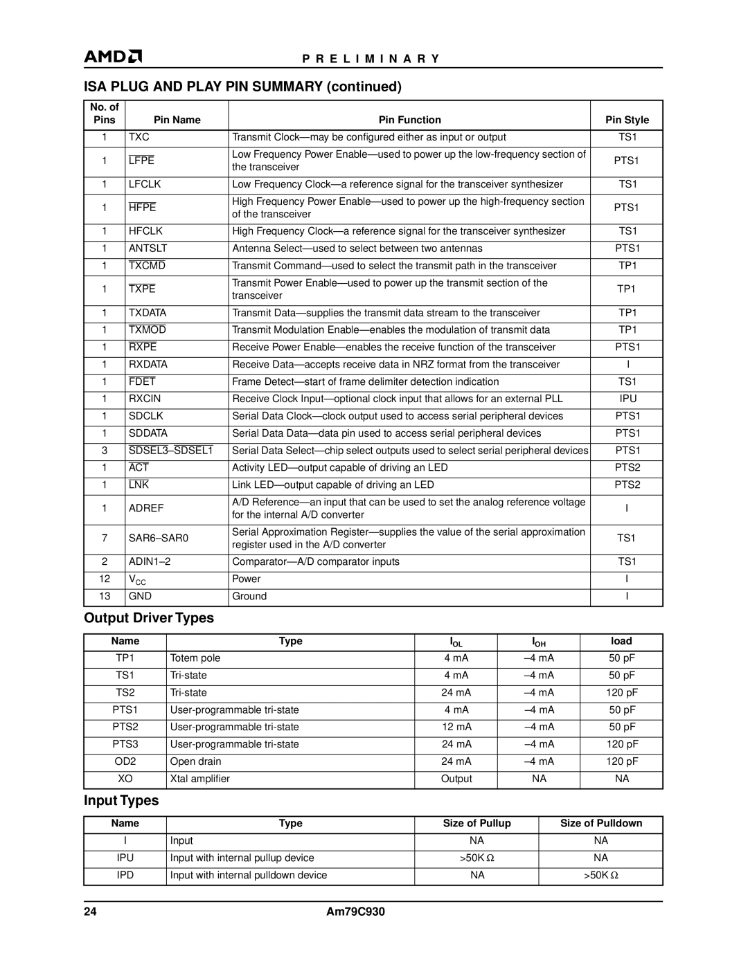
ISA PLUG AND PLAY PIN SUMMARY (continued)
No. of |
|
|
|
|
|
|
|
|
|
|
|
|
|
|
Pins |
|
|
| Pin Name | Pin Function | Pin Style | ||||||||
|
|
|
|
| ||||||||||
1 |
| TXC | Transmit | TS1 | ||||||||||
|
|
|
|
|
|
|
|
|
|
|
|
|
|
|
|
|
|
|
|
|
|
|
|
|
|
|
| Low Frequency Power |
|
1 |
| LFPE | PTS1 | |||||||||||
| the transceiver | |||||||||||||
|
|
|
|
|
|
|
|
|
|
|
|
|
| |
|
|
|
|
| ||||||||||
1 |
| LFCLK | Low Frequency | TS1 | ||||||||||
|
|
|
|
|
|
|
|
|
|
|
|
|
|
|
|
|
|
|
|
|
|
|
|
|
|
|
| High Frequency Power | PTS1 |
1 |
| HFPE | ||||||||||||
| of the transceiver | |||||||||||||
|
|
|
|
|
|
|
|
|
|
|
|
|
| |
|
|
|
|
| ||||||||||
1 |
| HFCLK | High Frequency | TS1 | ||||||||||
|
|
|
|
| ||||||||||
1 |
| ANTSLT | Antenna | PTS1 | ||||||||||
|
|
|
|
|
|
|
|
|
|
|
|
|
|
|
1 |
|
|
|
|
|
|
|
|
|
|
|
| Transmit | TP1 |
TXCMD | ||||||||||||||
|
|
|
|
|
|
|
|
|
|
|
|
|
|
|
|
|
|
|
|
|
|
|
|
|
|
|
| Transmit Power | TP1 |
1 |
| TXPE | ||||||||||||
| transceiver | |||||||||||||
|
|
|
|
|
|
|
|
|
|
|
|
|
| |
|
|
|
|
| ||||||||||
1 |
| TXDATA | Transmit | TP1 | ||||||||||
|
|
|
|
|
|
|
|
|
|
|
|
| ||
1 |
|
|
|
|
|
|
|
|
|
|
|
| Transmit Modulation | TP1 |
TXMOD | ||||||||||||||
|
|
|
|
|
|
|
|
|
|
|
| |||
1 |
|
|
|
|
|
|
|
|
|
| Receive Power | PTS1 | ||
RXPE | ||||||||||||||
|
|
|
|
| ||||||||||
1 |
| RXDATA | Receive | I | ||||||||||
|
|
|
|
|
|
|
|
|
|
| ||||
1 |
|
|
|
|
|
|
|
|
| Frame | TS1 | |||
FDET | ||||||||||||||
|
|
|
|
| ||||||||||
1 |
| RXCIN | Receive Clock | IPU | ||||||||||
|
|
|
|
| ||||||||||
1 |
| SDCLK | Serial Data | PTS1 | ||||||||||
|
|
|
|
| ||||||||||
1 |
| SDDATA | Serial Data | PTS1 | ||||||||||
|
|
|
|
|
|
|
|
| ||||||
3 |
|
|
|
|
|
|
|
|
|
|
|
| Serial Data | PTS1 |
| ||||||||||||||
|
|
|
|
|
|
| ||||||||
1 |
|
|
|
| Activity | PTS2 | ||||||||
ACT | ||||||||||||||
|
|
|
|
|
| |||||||||
1 |
|
|
| Link | PTS2 | |||||||||
LNK | ||||||||||||||
|
|
|
|
|
|
|
|
|
|
|
|
|
|
|
1 |
| ADREF | A/D | I | ||||||||||
| for the internal A/D converter | |||||||||||||
|
|
|
|
|
|
|
|
|
|
|
|
|
| |
|
|
|
|
|
|
|
|
|
|
|
|
|
|
|
7 |
|
| Serial Approximation | TS1 | ||||||||||
| register used in the A/D converter | |||||||||||||
|
|
|
|
|
|
|
|
|
|
|
|
|
| |
|
|
|
|
| ||||||||||
2 |
| TS1 | ||||||||||||
|
|
|
|
| ||||||||||
12 |
| VCC | Power | I | ||||||||||
13 |
| GND | Ground | I | ||||||||||
|
|
|
|
|
|
|
|
|
|
|
|
|
|
|
Output Driver Types
Name | Type | IOL | IOH | load |
TP1 | Totem pole | 4 mA | 50 pF | |
|
|
|
|
|
TS1 | 4 mA | 50 pF | ||
|
|
|
|
|
TS2 | 24 mA | 120 pF | ||
|
|
|
|
|
PTS1 | 4 mA | 50 pF | ||
|
|
|
|
|
PTS2 | 12 mA | 50 pF | ||
|
|
|
|
|
PTS3 | 24 mA | 120 pF | ||
|
|
|
|
|
OD2 | Open drain | 24 mA | 120 pF | |
|
|
|
|
|
XO | Xtal amplifier | Output | NA | NA |
|
|
|
|
|
Input Types |
|
|
|
|
Name | Type | Size of Pullup | Size of Pulldown |
|
|
|
|
I | Input | NA | NA |
|
|
|
|
IPU | Input with internal pullup device | >50K Ω | NA |
|
|
|
|
IPD | Input with internal pulldown device | NA | >50K Ω |
|
|
|
|
|
|
|
|
24 | Am79C930 |
|
|