Am79C930
Speed
Optional Processing
Operating Conditions
Package Type
Rxdata
Reset Pcmcia
Jtag Trst TMS/T3
Adref
INT1
Ireq
SIR0 MIR0 MIR1 SIR1 MIR15 SIR7
Srdy
MUX
IRQ
TIR0 TCR0
Fifo TIR31 TCR31
Table of Contents
E L I M I N a R Y AMD
RX Fifo
TX Fifo
TAP FSM
Register Descriptions
TIR31 Test
126
Absolute Maximum Ratings
AMD E L I M I N a R Y
Pcmcia Connection Diagram
Pin No Pin Name
Pin Name Pin No
No. Pins Pin Name Pin Function Pin Style
Txpe TP1
Lfpe PTS1
Hfpe PTS1
TP1, PTS1
Load
Name Type
Name Type Size of Pullup Size of Pulldown
DRQ0 Txcmd Ieee Memr
Reset LNK ACT CLK20 Test Pwrdwn
Ieee Sddata
Bale
ISA Plug and Play Connection Diagram
SD2 SD4
SD7
SD6
SD5
TCK Adref
SD5 Vsst Reset
SA1
ACT SDSEL2 ADIN1
PTS3/OD2
SD7-SD0
ISA Plug and Play PIN Summary
Pcmcia
Pins with Internal Pull Up or Pull Down Devices
Configuration Pins
PIN Descriptions
Input/Output
Host System Interface Pins
A14-0
D7-0
Iochrdy
Reset
AEN
Bale
IRQ4,5,9-12
MA16-0
MD7-0
RXC
Clkin
Pwrdwn
Rxcin
Rxdata
Hfclk
Lfclk
Llocke
Sddata
USER7
Adref
Sdclk
VDD5
TCK
Avss
TDI
VDDU2
VSS
VDDU1
VSSU1
Pin 45 STSCHG/BALE
Pin 1 USER2/LA19
Pin 2 USER3/SA16
Pin 3 USER4/LA17
Pin 92 USER7/IRQ11
Pin 91 USER1/IRQ12/EXTCTS/EXINT188
Pin 95 USER6/IRQ5/EXTSDF
Pin 94 RXC/IRQ10/EXTA2DST
Pin 96 USER5/IRQ4/EXTCHBSY
Pin 100 LNK
Pin 98 ACT
Pin 105 SDSEL2
Pin 101 Sdclk
Pin 102 Sddata
Pin 103 SDSEL3
Pin 122 Rxpe
Pin 115 TXC
Pin 118 Lfpe
Pin 120 Hfpe
Pin 132 Antslt
Pin 126 Txcmd
Pin 129 Txpe
Pin 131 Txmod
Pin 143 TXDATA/LA20
Pin 142 TXCMD/LA21
Pin 144 LLOCKE/SA15
Bus Interface Unit
Functional Description
Basic Functions
Detailed Functions
E L I M I N a R Y AMD
AMD E L I M I N a R Y
Embedded
Memory Interface
Medium Allocation
AMD E L I M I N a R Y
Transceiver Attachment Interface Unit Management
Flash Memory Management
Bus Interface Unit Interaction
Transceiver Attachment Interface Unit
TX Power Ramp Control
Tbclk = Tsclk X
Pin Timing Reference Name When RCEN=0 When RCEN=1
RX Data Parallelization
TX CRC Generation
TX Status
Start of Frame Delimiter Detection
Bit Ordering
RX Status Reporting
Rssi A/D Unit
Adda Enext Ensar UXA2DST
Physical Header Accommodation
DC Bias Control
Baud Determination Logic
Clear Channel Assessment Logic
Rssi = Rssi
Current CCA result is reported in the Chbsy bit of TIR26
Automatic Antenna Diversity Logic
Ubdcs Urssi
TXC As Input
Ieee 1149.1 Test Access Port Interface
Ubdsd Urssi Stpen
Instruction Register and Decoding Logic
Power Down Function
Boundary Scan Circuit
Supported Instructions
E L I M I N a R Y AMD
Software Access
Applicability to Ieee 802.11 Power Down Modes
Am79C930 System Interface Resources
Am79C930 Device Pcmcia Mode Common Memory Map
Am79C930 Device Pcmcia Mode Resource Requirements
Description of Reserved Use
Am79C930 Device Pcmcia Mode Common Memory Restricted Space
Pcmcia Address Size Physical Memory
SIR153
XXX
Am79C930 Device Pcmcia Mode Attribute Memory Map
Pcmcia Address Attribute Memory
ISA Plug and Play Mode Resources
Am79C930 Device Pcmcia Mode I/O MAP
Pcmcia
ISA Address in Memory SIR153 Size of Space Physical Memory
Am79C930 Device ISA Plug And Play Mode Memory Map
Kbytes of memory
Memory Range Memory Size
ISA Address Size Physical Memory
AMD E L I M I N a R Y
Resource Name
Am79C930 Device ISA Plug And Play Mode I/O MAP
Physical
ISA SIR1
Readdata
Port Name ISA Ieee P996 I/O Address Access
Address
Writedata
Address
ISA Plug and Play Plug and Play Port Register Name
MAC Firmware Resources
Physical Location of Memory
Active
INT0 TAI INT1 BIU
Interrupt Channel Allocation in the 80188 Core
Address Active Size
Interrupt Channel Interrupt Source
Loopback Operation
Reset Methods
Reset Pin
DMA Channel Allocation In The 80188 Core
Coreset SIR06
Register Descriptions
ISA PnP Reset
Sres TIR05
System Interface Registers SIR space
Bit Name Reset Value Description
SIR0 General Configuration Register GCR
SIR1 Bank Switching Select Register BSS
SIR3 Local Memory Address Register 148 LMA
Bit Name Reset Value Description IODPA70
MD70 during system interface accesses to Flash and Sram
SIR2 Local Memory Address Register 70 LMA
SIR5 I/O Data Port B Iodpb
MAC Interface Registers MIR Space
MIR0 Processor Interface Register PIR
MIR2 Power Down Length Count 70 Pdlc
MIR1 Power Up Clock Time 30 Puct
MIR5 Free Count 70 Fcnt
MIR3 Power Down Length Count 158 Pdlc
MIR4 Power Down Length Count 2216 Pdlc
Permarest
MIR9 TCR Mask Stschg Data
MIR8 Flash Wait States
Hostallow
FLASHWAIT10
Stschgd
SRAMWAIT10
Hostlongwait
Initdn
Undefined data
MIR10 Reserved
This register is reserved
Reserved. Must be written as a 0. Reads of this bit produce
Transceiver Attachment Interface Registers TIR Space
TIR Register Name
TIR
SIR110 ISA Plug Core
Play
SIR110 Core
TIR1 Network Status
TIR0 Network Control
TIR2 Serial Device
Antsw
TIR3 Fast Serial Port Control
TIR4 Interrupt Register
Chbsyc
TIR5 Interrupt Register
TIR7 Interrupt Unmask Register
TIR6 Interrupt Unmask Register
TIR8 Transmit Control
Txbsy
TIR9 Transmit Status
Txcrc
Txsdd
TIR11 Transmit Sequence Control
TIR13 Byte Count Register MSB
TIR12 Byte Count Register LSB
TIR14 Byte Count Limit LSB
TIR16 Receiver Control
TIR15 Byte Count Limit MSB
TIR17 Receive Status Register
TIR20 CRC32 Correct Byte Count LSB
Rxbsy
TIR18 RX Fifo Data Register
TIR19 Reserved
TIR22 CRC8 Correct Byte Count LSB
TIR21 CRC32 Correct Byte Count MSB
TIR23 CRC8 Correct Byte Count MSB
TIR24 TCR Index Register
TIR25 Configuration Data Port
Bit Name Reset Value Description CD70
By the current setting of the Configuration Index Register
TIR27 Serial Approximation Register
Adda
Srcs
Strtc
TIR30 Test Dummy Register
Bit Name Reset Value
TIR28 Rssi Lower Limit
TIR29 User Pin Data
TCR0 Network Configuration
TAI Configuration Register Space TCR
These bit must be set to 0. Do not write to this register
01h Bit Name Reset Value Description
TCR1 Transmit Configuration
Am79C930 105
03h
TCR2 Clock Recovery
TCR3 Receive Configuration
02h
05h
TCR4 Antenna Diversity Timer
04h
TCR5 TX Ramp Up Timing
07h
TCR6 TX Ramp Down Timing
06h
TCR7 Pin Data a
Txdatald
U1INTCNT
Txcmdt
Antsltld
08h
Bit Name Reset Value Description SDLT70 00h
Bit Name Reset Value Description SDLT158 00h
TCR8 Start Delimiter LSB
0Ch
TCR11 Interrupt Register
0Bh
TCR12 Interrupt Unmask Register
0Eh
TCR13 Pin Configuration a
TCR14 Pin Configuration B
0Dh
0Fh
TCR15 Pin Configuration C
Am79C930 113
10h
Acten
Stschgfn
TCR16 Baud Detect Start
TCR18 Baud Detect Upper Limit
11h Bit Name Reset Value Description
12h Bit Name Reset Value Description
Undefined data BDLLT50
TCR20 Baud Detect Accept Count for Stop Diversity
TCR19 Baud Detect Accept Count for Carrier Sense
13h
BDCS50
TCR23 Baud Detect Fail Count
15h Bit Name Reset Value Description BDRN30
TCR22 Baud Detect Accept Count
16h
19h
TCR25 Rssi Configuration
18h
SS50 00h
CACT=TIR277
Analog-to-Digital State Machine Timing Am79C930 119
1Ah
TCR26 Reserved
1Bh
1Ch Bit Name Reset Value Description
TCR28 Clear Channel Assessment Configuration
Am79C930 121
1Dh
TCR29 Reserved
1Eh
1Fh Description
TCR31 Device Revision
Am79C930 123
Pcmcia CCR Registers and Pcmcia CIS Space
Pcmcia Configuration Option Register
Sreset
Pcmcia Card Configuration and Status Register
Am79C930 125
Vice actually enters the power down mode Interrupt
Til the interrupt has been serviced not pulse generated
Pcmcia Card Information Structure CIS
Commercial C Devices
DC Characteristics
Am79C930 DC Characteristics
Absolute Maximum Ratings Operating Ranges
Am79C930 127
DC Characteristics Am79C930 DC Characteristics
Parameter Description Test Conditions Min Max
To 3.6
Temperature TA C to + 70C Supply Voltages
Absolute Maximum Ratings
VDDP, VDD5
Am79C930 129
130
Ieee 1149.1 DC Characteristics 5.0 and 3.3
Am79C930 131
Pcmcia Memory Read Access
Unit
132
Pcmcia Memory Write Access
Am79C930 133
Pcmcia I/O Read Access
134
Pcmcia I/O Write Access
Am79C930 135
136
ISA Access
Am79C930 137
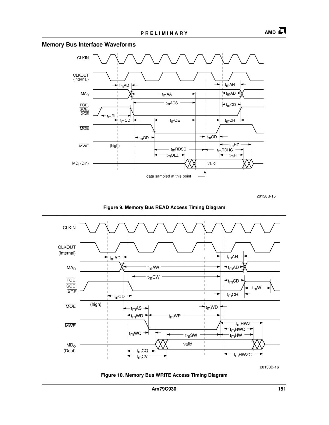
Memory BUS Read Access
138
Memory BUS Write Access
Am79C930 139
140
Am79C930 141
AC Characteristics TAI Interface Absolute Maximum Ratings
Max Unit
TAI Interface AC Characteristics
142
Am79C930 143
144
Am79C930 145
146
Clkin ↓
Am79C930 147
ANALOG-TO-DIGITAL A/D Converter Characteristics
TCK −
Din
Timing Waveforms
Pcmcia Bus Interface Waveforms
REG
Pcmcia I/O Read Access Timing Diagram
150
ISA Bus Interface Waveforms
Clkin Clkout
Memory Bus Interface Waveforms
152
Clock Waveforms
ICO
TAI Waveforms
RCO
154
Programmable Interface Waveforms
Am79C930 155
Ieee 1149.1 Interface Waveforms
TDI, TMS
Pcmcia AC Test Reference Waveform
AC Test Reference Waveforms
156
V Non-PCMCIA AC Test Reference Waveform
NON-PCMCIA AC Test Reference Waveform
PQT144 Pin Thin Quad Flat Pack measured in millimeters
Physical Dimensions
158
Typical Am79C930 System Application
Device Configuration
Frame Reception
Frame Transmission
Trademarks