AMDP R E L I M I N A R Y
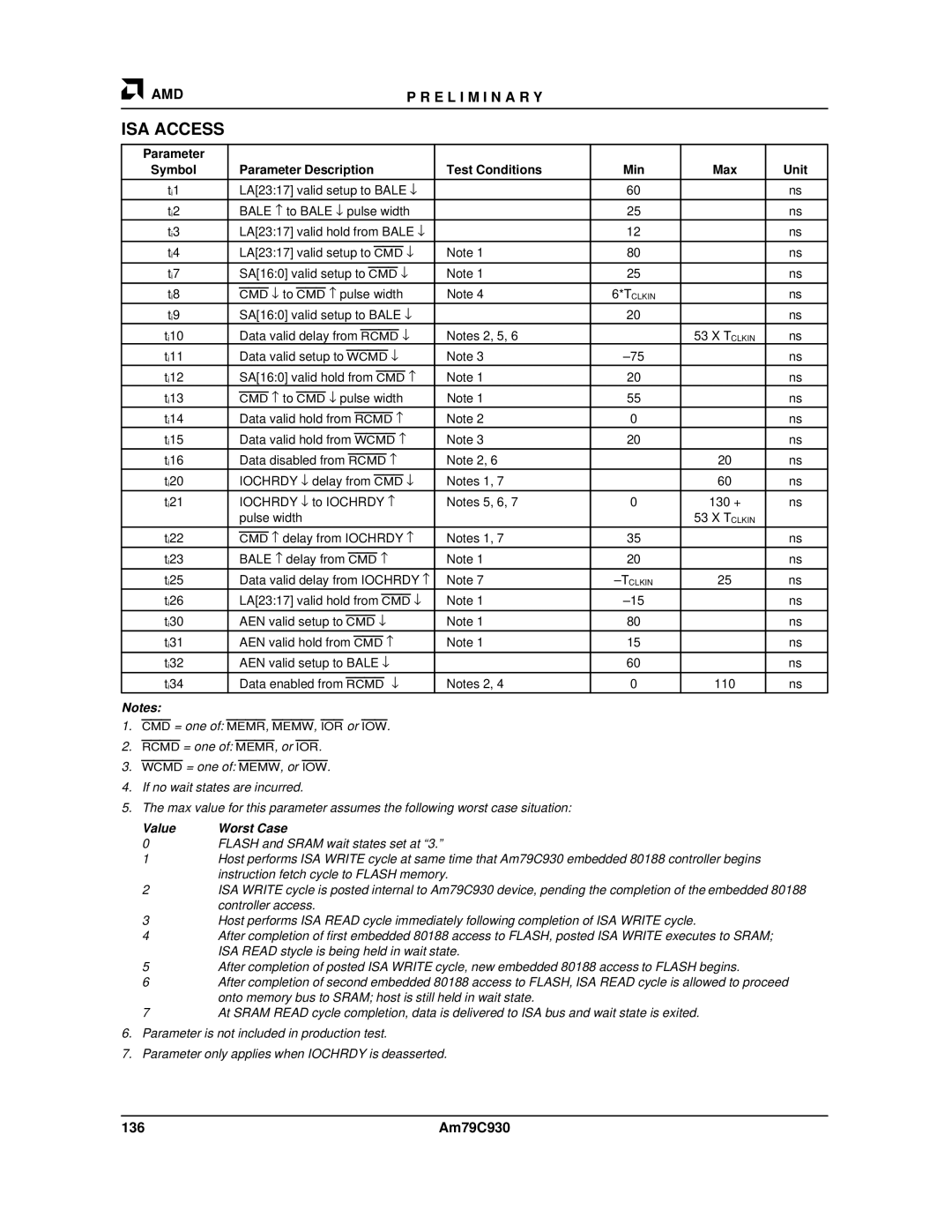
ISA ACCESS
Parameter |
|
|
|
|
|
Symbol | Parameter Description | Test Conditions | Min | Max | Unit |
|
|
|
|
|
|
ti1 | LA[23:17] valid setup to BALE ↓ |
| 60 |
| ns |
|
|
|
|
|
|
ti2 | BALE − to BALE ↓ pulse width |
| 25 |
| ns |
ti3 | LA[23:17] valid hold from BALE ↓ |
| 12 |
| ns |
ti4 | LA[23:17] valid setup to CMD ↓ | Note 1 | 80 |
| ns |
|
|
|
|
|
|
ti7 | SA[16:0] valid setup to CMD ↓ | Note 1 | 25 |
| ns |
|
|
|
|
|
|
ti8 | CMD ↓ to CMD − pulse width | Note 4 | 6*TCLKIN |
| ns |
ti9 | SA[16:0] valid setup to BALE ↓ |
| 20 |
| ns |
ti10 | Data valid delay from RCMD ↓ | Notes 2, 5, 6 |
| 53 X TCLKIN | ns |
ti11 | Data valid setup to WCMD ↓ | Note 3 |
| ns | |
ti12 | SA[16:0] valid hold from CMD − | Note 1 | 20 |
| ns |
ti13 | CMD − to CMD ↓ pulse width | Note 1 | 55 |
| ns |
ti14 | Data valid hold from RCMD − | Note 2 | 0 |
| ns |
ti15 | Data valid hold from WCMD − | Note 3 | 20 |
| ns |
ti16 | Data disabled from RCMD − | Note 2, 6 |
| 20 | ns |
ti20 | IOCHRDY ↓ delay from CMD ↓ | Notes 1, 7 |
| 60 | ns |
|
|
|
|
|
|
ti21 | IOCHRDY ↓ to IOCHRDY − | Notes 5, 6, 7 | 0 | 130 + | ns |
| pulse width |
|
| 53 X TCLKIN |
|
ti22 | CMD − delay from IOCHRDY − | Notes 1, 7 | 35 |
| ns |
ti23 | BALE − delay from CMD − | Note 1 | 20 |
| ns |
|
|
|
|
|
|
ti25 | Data valid delay from IOCHRDY − | Note 7 | 25 | ns | |
ti26 | LA[23:17] valid hold from CMD ↓ | Note 1 |
| ns | |
|
|
|
|
|
|
ti30 | AEN valid setup to CMD ↓ | Note 1 | 80 |
| ns |
ti31 | AEN valid hold from CMD − | Note 1 | 15 |
| ns |
|
|
|
|
|
|
ti32 | AEN valid setup to BALE ↓ |
| 60 |
| ns |
|
|
|
|
|
|
ti34 | Data enabled from RCMD ↓ | Notes 2, 4 | 0 | 110 | ns |
Notes:
1.CMD = one of: MEMR, MEMW, IOR or IOW.
2.RCMD = one of: MEMR, or IOR.
3.WCMD = one of: MEMW, or IOW.
4.If no wait states are incurred.
5.The max value for this parameter assumes the following worst case situation:
Value | Worst Case |
0FLASH and SRAM wait states set at “3.”
1Host performs ISA WRITE cycle at same time that Am79C930 embedded 80188 controller begins instruction fetch cycle to FLASH memory.
2ISA WRITE cycle is posted internal to Am79C930 device, pending the completion of the embedded 80188 controller access.
3Host performs ISA READ cycle immediately following completion of ISA WRITE cycle.
4After completion of first embedded 80188 access to FLASH, posted ISA WRITE executes to SRAM; ISA READ stycle is being held in wait state.
5After completion of posted ISA WRITE cycle, new embedded 80188 access to FLASH begins.
6After completion of second embedded 80188 access to FLASH, ISA READ cycle is allowed to proceed onto memory bus to SRAM; host is still held in wait state.
7At SRAM READ cycle completion, data is delivered to ISA bus and wait state is exited.
6.Parameter is not included in production test.
7.Parameter only applies when IOCHRDY is deasserted.
136 | Am79C930 |