| P R E L I M I N A R Y |
|
|
|
| AMD | |||
|
|
|
|
|
|
|
|
|
|
|
|
|
|
|
|
|
|
|
|
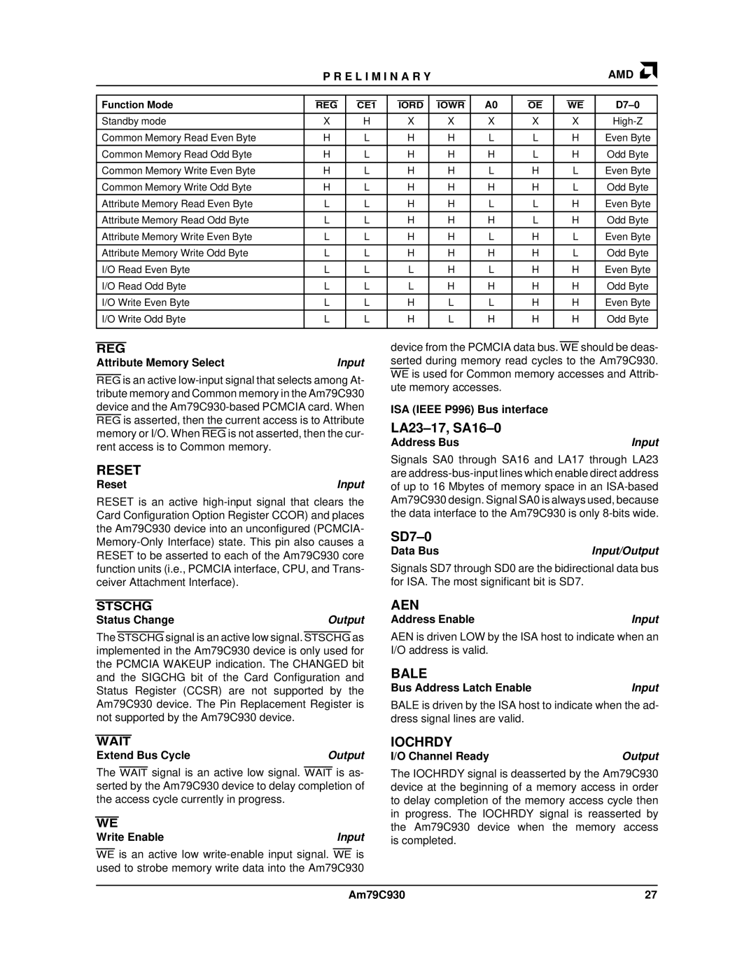
Function Mode | REG | CE1 | IORD |
| IOWR | A0 | OE | WE | |
|
|
|
|
|
|
|
|
|
|
Standby mode | X | H | X |
| X | X | X | X | |
|
|
|
|
|
|
|
|
|
|
Common Memory Read Even Byte | H | L | H |
| H | L | L | H | Even Byte |
Common Memory Read Odd Byte | H | L | H |
| H | H | L | H | Odd Byte |
|
|
|
|
|
|
|
|
|
|
Common Memory Write Even Byte | H | L | H |
| H | L | H | L | Even Byte |
|
|
|
|
|
|
|
|
|
|
Common Memory Write Odd Byte | H | L | H |
| H | H | H | L | Odd Byte |
|
|
|
|
|
|
|
|
|
|
Attribute Memory Read Even Byte | L | L | H |
| H | L | L | H | Even Byte |
|
|
|
|
|
|
|
|
|
|
Attribute Memory Read Odd Byte | L | L | H |
| H | H | L | H | Odd Byte |
Attribute Memory Write Even Byte | L | L | H |
| H | L | H | L | Even Byte |
|
|
|
|
|
|
|
|
|
|
Attribute Memory Write Odd Byte | L | L | H |
| H | H | H | L | Odd Byte |
|
|
|
|
|
|
|
|
|
|
I/O Read Even Byte | L | L | L |
| H | L | H | H | Even Byte |
I/O Read Odd Byte | L | L | L |
| H | H | H | H | Odd Byte |
|
|
|
|
|
|
|
|
|
|
I/O Write Even Byte | L | L | H |
| L | L | H | H | Even Byte |
I/O Write Odd Byte | L | L | H |
| L | H | H | H | Odd Byte |
|
|
|
|
|
|
|
|
|
|
REG
Attribute Memory Select | Input |
REG is an active
RESET
Reset | Input |
RESET is an active
device from the PCMCIA data bus. WE should be deas- serted during memory read cycles to the Am79C930. WE is used for Common memory accesses and Attrib- ute memory accesses.
ISA (IEEE P996) Bus interface
LA23–17, SA16–0
Address Bus | Input |
Signals SA0 through SA16 and LA17 through LA23 are
SD7–0
Data Bus | Input/Output |
Signals SD7 through SD0 are the bidirectional data bus for ISA. The most significant bit is SD7.
STSCHG
Status Change | Output |
The STSCHG signal is an active low signal. STSCHG as implemented in the Am79C930 device is only used for the PCMCIA WAKEUP indication. The CHANGED bit and the SIGCHG bit of the Card Configuration and Status Register (CCSR) are not supported by the Am79C930 device. The Pin Replacement Register is not supported by the Am79C930 device.
WAIT
Extend Bus Cycle | Output |
The WAIT signal is an active low signal. WAIT is as- serted by the Am79C930 device to delay completion of the access cycle currently in progress.
WE
Write Enable | Input |
WE is an active low
AEN
Address Enable | Input |
AEN is driven LOW by the ISA host to indicate when an I/O address is valid.
BALE
Bus Address Latch Enable | Input |
BALE is driven by the ISA host to indicate when the ad- dress signal lines are valid.
IOCHRDY
I/O Channel Ready | Output |
The IOCHRDY signal is deasserted by the Am79C930 device at the beginning of a memory access in order to delay completion of the memory access cycle then in progress. The IOCHRDY signal is reasserted by the Am79C930 device when the memory access is completed.
Am79C930 | 27 |