AMD |
| P R E L I M I N A R Y | |
|
|
|
|
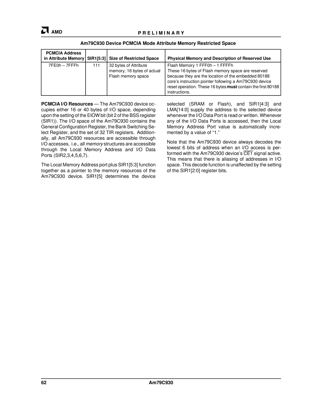
Am79C930 Device PCMCIA Mode Attribute Memory Restricted Space | |||
|
|
|
|
PCMCIA Address |
|
|
|
in Attribute Memory | SIR1[5:3] | Size of Restricted Space | Physical Memory and Description of Reserved Use |
|
|
|
|
7FE0h – 7FFFh | 111 | 32 bytes of Attribute | Flash Memory 1 FFF0h – 1 FFFFh |
|
| memory, 16 bytes of actual | These 16 bytes of Flash memory space are reserved |
|
| Flash memory space | because they are the location of the embedded 80188 |
|
|
| core's instruction pointer following a Am79C930 device |
|
|
| reset operation. These 16 bytes must contain the first 80188 |
|
|
| instructions. |
|
|
|
|
PCMCIA I/O Resources — The Am79C930 device oc- cupies either 16 or 40 bytes of I/O space, depending upon the setting of the EIOW bit (bit 2 of the BSS register (SIR1)). The I/O space of the Am79C930 contains the General Configuration Register, the Bank Switching Se- lect Register, and the set of 32 TIR registers. Addition- ally, all Am79C930 resources are accessible through I/O accesses, i.e., all memory structures are accessible through the Local Memory Address and I/O Data Ports (SIR2,3,4,5,6,7).
The Local Memory Address port plus SIR1[5:3] function together as a pointer to the memory resources of the Am79C930 device. SIR1[5] determines the device
selected (SRAM or Flash), and SIR1[4:3] and LMA[14:0] supply the address to the selected device whenever the I/O Data Port is read or written. Whenever any of the I/O Data Ports is accessed, then the Local Memory Address Port value is automatically incre- mented by a value of “1.”
Note that the Am79C930 device always decodes the lowest 6 bits of address when an I/O access is per- formed with the Am79C930 device's CE1 signal active. This means that there is aliasing of addresses in I/O space. This decode function is unaffected by the setting of the SIR1[2:0] register bits.
62 | Am79C930 |