AMD | P R E L I M I N A R Y |
|
|
The following is a brief summary of the IEEE 1149.1 compatible test functions implemented in the Am79C930 device:
Boundary Scan Circuit
The boundary scan test circuit uses five pins: TRST, TCK, TMS, TDI, and TDO. These five pins are collec- tively labeled the TAP. The boundary scan test circuit in- cludes a finite state machine (FSM), an instruction register, and a data register array. Internal
TAP FSM
The TAP engine is a
Supported Instructions
In addition to the minimum IEEE 1149.1 requirements (BYPASS, EXTEST, and SAMPLE instructions), one additional instruction (IDCODE) is provided as addi- tional support for board level testing. All unused instruc- tion decodes are reserved.
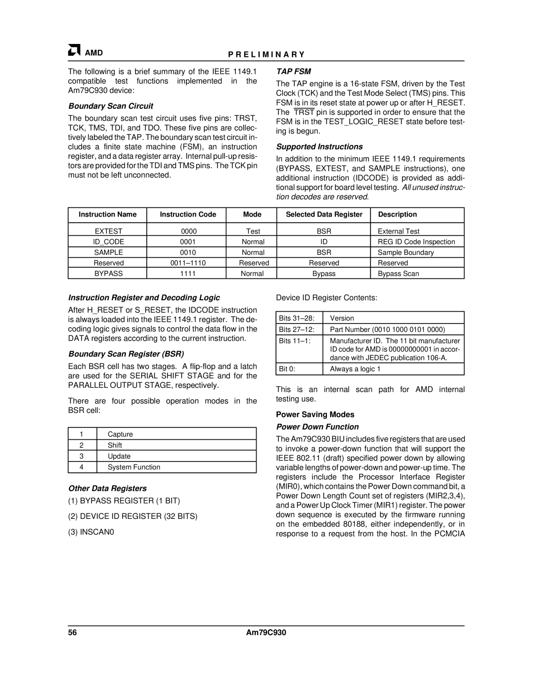
Instruction Name | Instruction Code | Mode | Selected Data Register | Description |
|
|
|
|
|
EXTEST | 0000 | Test | BSR | External Test |
ID_CODE | 0001 | Normal | ID | REG ID Code Inspection |
SAMPLE | 0010 | Normal | BSR | Sample Boundary |
Reserved | Reserved | Reserved | Reserved | |
BYPASS | 1111 | Normal | Bypass | Bypass Scan |
Instruction Register and Decoding Logic
After H_RESET or S_RESET, the IDCODE instruction is always loaded into the IEEE 1149.1 register. The de- coding logic gives signals to control the data flow in the DATA registers according to the current instruction.
Boundary Scan Register (BSR)
Each BSR cell has two stages. A
There are four possible operation modes in the BSR cell:
1Capture
2Shift
3Update
4System Function
Other Data Registers
(1)BYPASS REGISTER (1 BIT)
(2)DEVICE ID REGISTER (32 BITS)
(3)INSCAN0
Device ID Register Contents:
Bits | Version |
|
|
Bits | Part Number (0010 1000 0101 0000) |
Bits | Manufacturer ID. The 11 bit manufacturer |
| ID code for AMD is 00000000001 in accor- |
| dance with JEDEC publication |
Bit 0: | Always a logic 1 |
|
|
This is an internal scan path for AMD internal testing use.
Power Saving Modes
Power Down Function
The Am79C930 BIU includes five registers that are used to invoke a
56 | Am79C930 |