AMDP R E L I M I N A R Y
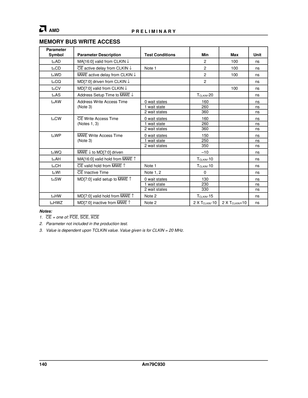
MEMORY BUS WRITE ACCESS
Parameter |
|
|
|
|
|
Symbol | Parameter Description | Test Conditions | Min | Max | Unit |
|
|
|
|
|
|
tmAD | MA[16:0] valid from CLKIN ↓ |
| 2 | 100 | ns |
|
|
|
|
|
|
tmCD | CE active delay from CLKIN ↓ | Note 1 | 2 | 100 | ns |
tmWD | MWE active delay from CLKIN ↓ |
| 2 | 100 | ns |
tmCQ | MD[7:0] driven from CLKIN ↓ |
| 2 |
| ns |
|
|
|
|
|
|
tmCV | MD[7:0] valid from CLKIN ↓ |
|
| 100 | ns |
|
|
|
|
|
|
tmAS | Address Setup Time to MWE ↓ |
|
| ns | |
tmAW | Address Write Access Time | 0 wait states | 160 |
| ns |
| (Note 3) | 1 wait state | 260 |
| ns |
|
| 2 wait states | 360 |
| ns |
tmCW | CE Write Access Time | 0 wait states | 160 |
| ns |
| (Notes 1, 3) | 1 wait state | 260 |
| ns |
|
| 2 wait states | 360 |
| ns |
tmWP | MWE Write Access Time | 0 wait states | 150 |
| ns |
| (Note 3) | 1 wait state | 250 |
| ns |
|
| 2 wait states | 350 |
| ns |
tmWQ | MWE ↓ to MD[7:0] driven |
|
| ns | |
tmAH | MA[16:0] valid hold from MWE − |
|
| ns | |
tmCH | CE valid hold from MWE − | Note 1 |
| ns | |
|
|
|
|
|
|
tmWI | CE Inactive Time | Note 1, 2 | 0 |
| ns |
tmSW | MD[7:0] valid setup to MWE − | 0 wait states | 130 |
| ns |
|
| 1 wait state | 230 |
| ns |
|
| 2 wait states | 330 |
| ns |
tmHW | MD[7:0] valid hold from MWE − | Note 2 |
| ns | |
tmHWZ | MD[7:0] inactive from MWE − | Note 2 | 2 X | 2 X TCLKIN+10 | ns |
|
|
|
|
|
|
Notes:
1.CE = one of: FCE, SCE, XCE
2.Parameter not included in the production test.
3.Value is dependent upon TCLKIN value. Value given is for CLKIN = 20 MHz.
140 | Am79C930 |