|
|
| P R E L I M I N A R Y | AMD | |
|
|
|
|
| |
|
|
| value that is present on the LLOCKE pin, regardless of the setting of | ||
|
|
| the PCMCIA pin. |
|
|
|
|
| The control of the function of the LLOCKE/SA15 pin is described in | ||
|
|
| the |
|
|
5 | Reserved | – | Reserved. Must be written as a 0. Reads of these bits produce | ||
|
|
| undefined data. |
|
|
4:0 | USEREN[4:0] | 00h | USER[4:0] Enable. These five bits are used to determine the direc- | ||
|
|
| tion of the USER[4:0] pins. When any bit of the USEREN register is | ||
|
|
| set to a 1, then the corresponding USER device pin is enabled to | ||
|
|
| drive both high and low output values. USER output values are de- | ||
|
|
| termined by the individual bit settings of the USERDT register | ||
|
|
| (TIR29). When any bit of the USEREN register is reset to a 0, then | ||
|
|
| the corresponding USER device pin is forced to a | ||
|
|
| state. Reads of the USERDT register (TIR29) will yield the value | ||
|
|
| that is present on any particular USER pin. |
|
|
The control of the function of each of the USER pins is described in the
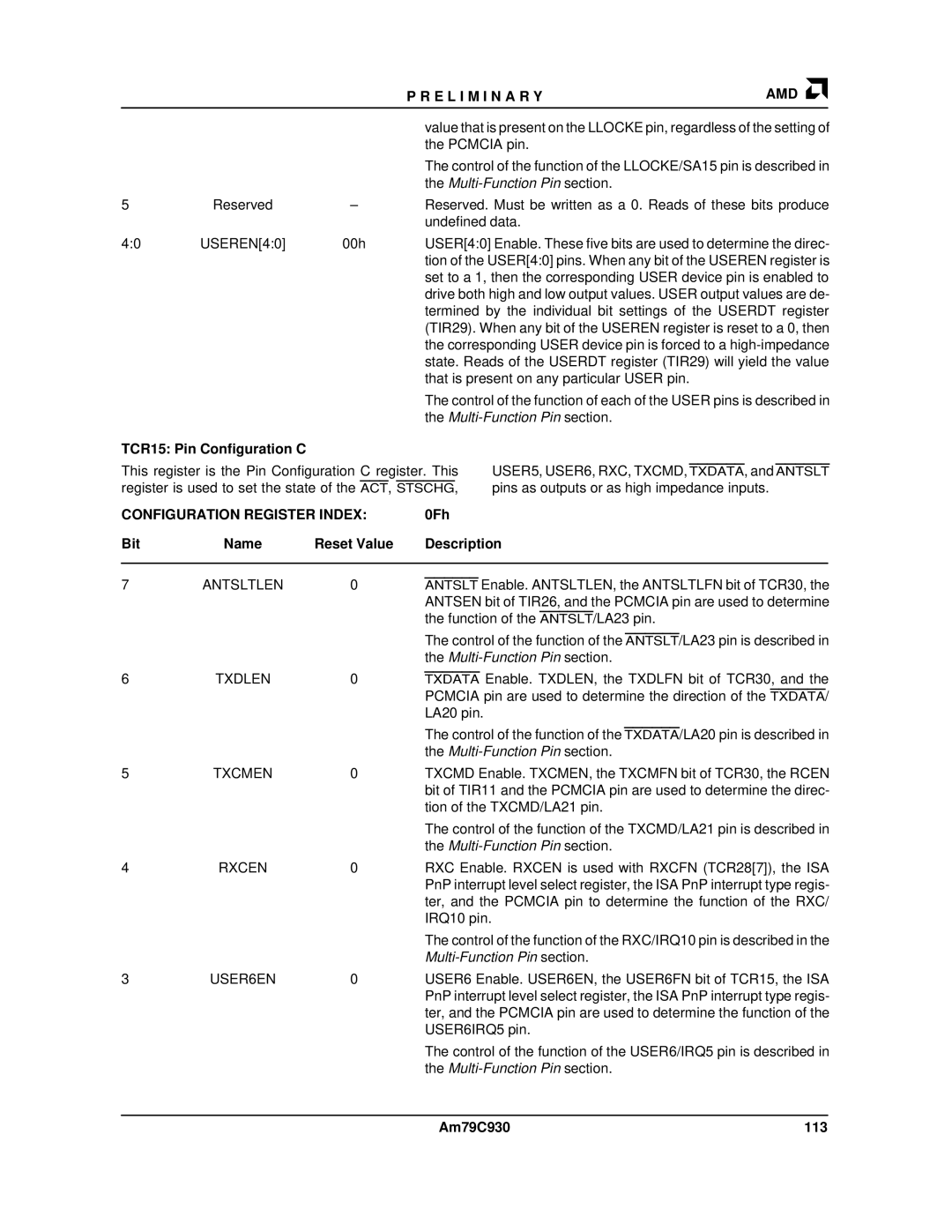
TCR15: Pin Configuration C
This register is the Pin Configuration C register. This register is used to set the state of the ACT, STSCHG,
CONFIGURATION REGISTER INDEX: | 0Fh |
USER5, USER6, RXC, TXCMD, TXDATA, and ANTSLT pins as outputs or as high impedance inputs.
Bit | Name | Reset Value | Description |
|
|
|
|
|
|
| |
7 | ANTSLTLEN | 0 | ANTSLT Enable. ANTSLTLEN, the ANTSLTLFN bit of TCR30, the | ||
|
|
| ANTSEN bit of TIR26, and the PCMCIA pin are used to determine | ||
|
|
| the function of the ANTSLT/LA23 pin. |
|
|
|
|
| The control of the function of the ANTSLT/LA23 pin is described in | ||
|
|
| the |
|
|
6 | TXDLEN | 0 | TXDATA Enable. TXDLEN, the TXDLFN bit of TCR30, and the | ||
|
|
| PCMCIA pin are used to determine the direction of the TXDATA/ | ||
|
|
| LA20 pin. |
|
|
|
|
| The control of the function of the TXDATA/LA20 pin is described in | ||
|
|
| the |
|
|
5 | TXCMEN | 0 | TXCMD Enable. TXCMEN, the TXCMFN bit of TCR30, the RCEN | ||
|
|
| bit of TIR11 and the PCMCIA pin are used to determine the direc- | ||
|
|
| tion of the TXCMD/LA21 pin. |
|
|
|
|
| The control of the function of the TXCMD/LA21 pin is described in | ||
|
|
| the |
|
|
4 | RXCEN | 0 | RXC Enable. RXCEN is used with RXCFN (TCR28[7]), the ISA | ||
|
|
| PnP interrupt level select register, the ISA PnP interrupt type regis- | ||
|
|
| ter, and the PCMCIA pin to determine the function of the RXC/ | ||
|
|
| IRQ10 pin. |
|
|
|
|
| The control of the function of the RXC/IRQ10 pin is described in the | ||
|
|
|
|
|
|
3 | USER6EN | 0 | USER6 Enable. USER6EN, the USER6FN bit of TCR15, the ISA | ||
|
|
| PnP interrupt level select register, the ISA PnP interrupt type regis- | ||
|
|
| ter, and the PCMCIA pin are used to determine the function of the | ||
|
|
| USER6IRQ5 pin. |
|
|
|
|
| The control of the function of the USER6/IRQ5 pin is described in | ||
|
|
| the |
|
|
|
|
|
|
|
|
|
|
| Am79C930 | 113 | |
