P R E L I M I N A R Y | AMD |
|
|
to TIR10. It is also possible to use 80188 MOV instruc- tions to unload RX data from the RX FIFO. The RX FIFO may be unloaded by reading from TIR18.
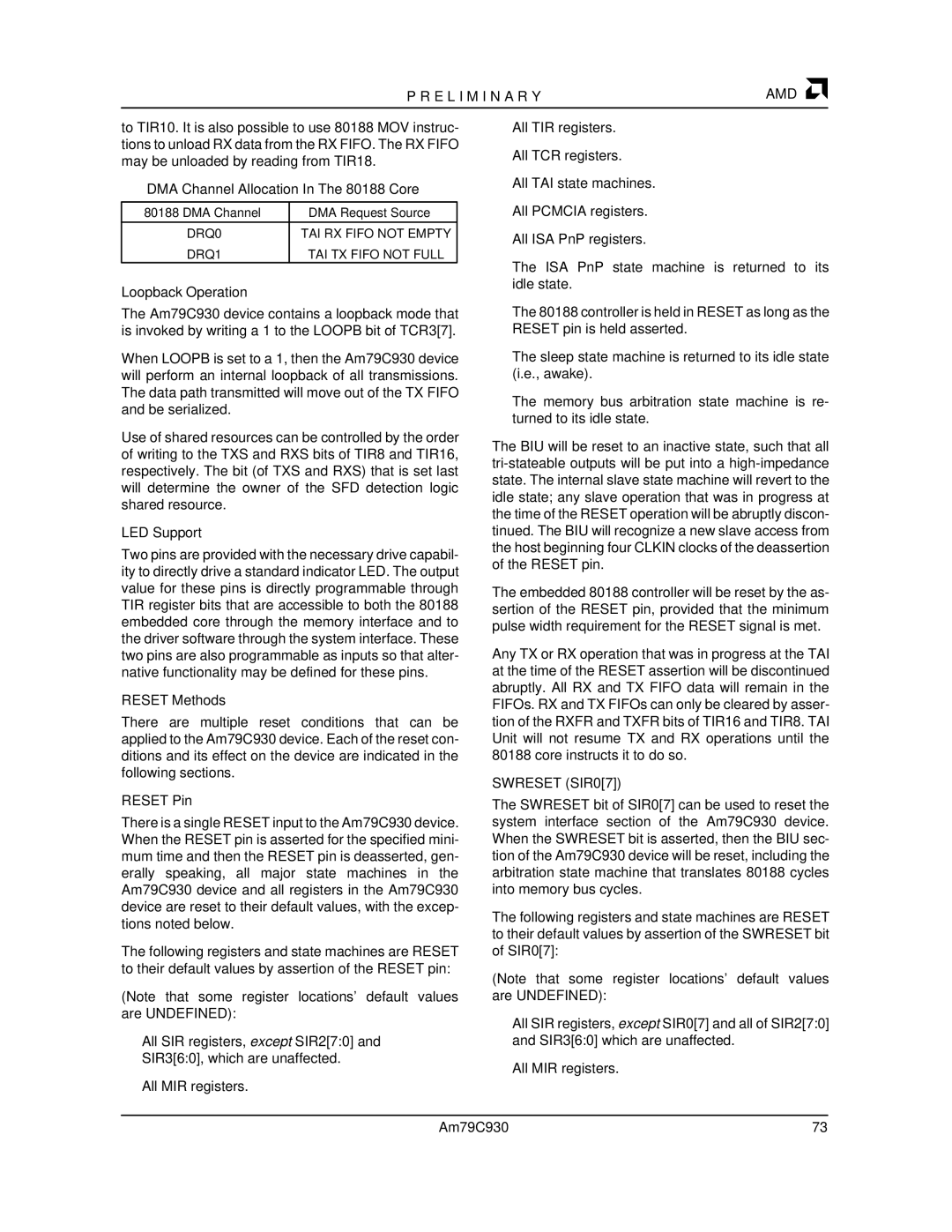
DMA Channel Allocation In The 80188 Core
80188 DMA Channel | DMA Request Source |
|
|
DRQ0 | TAI RX FIFO NOT EMPTY |
DRQ1 | TAI TX FIFO NOT FULL |
Loopback Operation
The Am79C930 device contains a loopback mode that is invoked by writing a 1 to the LOOPB bit of TCR3[7].
When LOOPB is set to a 1, then the Am79C930 device will perform an internal loopback of all transmissions. The data path transmitted will move out of the TX FIFO and be serialized.
Use of shared resources can be controlled by the order of writing to the TXS and RXS bits of TIR8 and TIR16, respectively. The bit (of TXS and RXS) that is set last will determine the owner of the SFD detection logic shared resource.
LED Support
Two pins are provided with the necessary drive capabil- ity to directly drive a standard indicator LED. The output value for these pins is directly programmable through TIR register bits that are accessible to both the 80188 embedded core through the memory interface and to the driver software through the system interface. These two pins are also programmable as inputs so that alter- native functionality may be defined for these pins.
RESET Methods
There are multiple reset conditions that can be applied to the Am79C930 device. Each of the reset con- ditions and its effect on the device are indicated in the following sections.
All TIR registers.
All TCR registers.
All TAI state machines.
All PCMCIA registers.
All ISA PnP registers.
The ISA PnP state machine is returned to its idle state.
The 80188 controller is held in RESET as long as the RESET pin is held asserted.
The sleep state machine is returned to its idle state (i.e., awake).
The memory bus arbitration state machine is re- turned to its idle state.
The BIU will be reset to an inactive state, such that all
The embedded 80188 controller will be reset by the as- sertion of the RESET pin, provided that the minimum pulse width requirement for the RESET signal is met.
Any TX or RX operation that was in progress at the TAI at the time of the RESET assertion will be discontinued abruptly. All RX and TX FIFO data will remain in the FIFOs. RX and TX FIFOs can only be cleared by asser- tion of the RXFR and TXFR bits of TIR16 and TIR8. TAI Unit will not resume TX and RX operations until the 80188 core instructs it to do so.
SWRESET (SIR0[7])
RESET Pin
There is a single RESET input to the Am79C930 device. When the RESET pin is asserted for the specified mini- mum time and then the RESET pin is deasserted, gen- erally speaking, all major state machines in the Am79C930 device and all registers in the Am79C930 device are reset to their default values, with the excep- tions noted below.
The following registers and state machines are RESET to their default values by assertion of the RESET pin:
(Note that some register locations' default values are UNDEFINED):
All SIR registers, except SIR2[7:0] and
SIR3[6:0], which are unaffected.
All MIR registers.
The SWRESET bit of SIR0[7] can be used to reset the system interface section of the Am79C930 device. When the SWRESET bit is asserted, then the BIU sec- tion of the Am79C930 device will be reset, including the arbitration state machine that translates 80188 cycles into memory bus cycles.
The following registers and state machines are RESET to their default values by assertion of the SWRESET bit of SIR0[7]:
(Note that some register locations' default values are UNDEFINED):
All SIR registers, except SIR0[7] and all of SIR2[7:0] and SIR3[6:0] which are unaffected.
All MIR registers.
Am79C930 | 73 |