P R E L I M I N A R Y
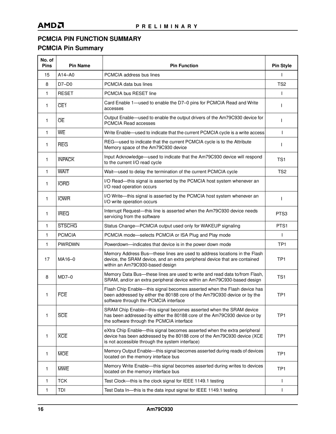
PCMCIA PIN FUNCTION SUMMARY
PCMCIA Pin Summary
No. of |
|
|
|
|
|
|
|
|
|
|
|
|
|
|
Pins |
|
|
|
|
|
| Pin Name | Pin Function | Pin Style | |||||
|
|
|
|
| ||||||||||
15 |
| PCMCIA address bus lines | I | |||||||||||
|
|
|
|
| ||||||||||
8 |
| PCMCIA data bus lines | TS2 | |||||||||||
|
|
|
|
| ||||||||||
1 |
| RESET | PCMCIA bus RESET line | I | ||||||||||
|
|
|
|
|
|
|
|
|
|
|
|
|
|
|
|
|
|
|
|
|
|
|
|
|
|
|
| Card Enable |
|
1 |
| CE1 | I | |||||||||||
| accesses | |||||||||||||
|
|
|
|
|
|
|
|
|
|
|
|
|
| |
|
|
|
|
|
|
|
|
|
|
|
|
|
|
|
|
|
|
|
|
|
|
|
|
|
|
|
| Output |
|
1 |
| OE | I | |||||||||||
| PCMCIA Read accesses | |||||||||||||
|
|
|
|
|
|
|
|
|
|
|
|
|
| |
|
|
|
|
|
|
|
|
|
|
|
|
|
| |
1 |
|
|
|
|
|
|
|
|
|
|
|
| Write | I |
WE | ||||||||||||||
|
|
|
|
|
|
|
|
|
|
|
|
|
|
|
|
|
|
|
|
|
|
|
|
|
|
|
|
| |
1 |
| REG | I | |||||||||||
| Memory space of the Am79C930 device | |||||||||||||
|
|
|
|
|
|
|
|
|
|
|
|
|
| |
|
|
|
|
|
|
|
|
|
|
|
|
|
|
|
|
|
|
|
|
|
|
|
|
|
|
|
| Input |
|
1 |
| INPACK | TS1 | |||||||||||
| to the current I/O read cycle | |||||||||||||
|
|
|
|
|
|
|
|
|
|
|
|
|
| |
|
|
|
|
|
|
|
|
|
|
|
| |||
1 |
|
|
|
|
|
|
|
|
|
|
| TS2 | ||
WAIT | ||||||||||||||
|
|
|
|
|
|
|
|
|
|
|
|
|
|
|
|
|
|
|
|
|
|
|
|
|
|
|
| I/O |
|
1 |
| IORD |
| |||||||||||
| I/O read operation occurs |
| ||||||||||||
|
|
|
|
|
|
|
|
|
|
|
|
|
| |
|
|
|
|
|
|
|
|
|
|
|
|
|
|
|
|
|
|
|
|
|
|
|
|
|
|
|
| I/O |
|
1 |
| IOWR | I | |||||||||||
| I/O write operation occurs | |||||||||||||
|
|
|
|
|
|
|
|
|
|
|
|
|
| |
|
|
|
|
|
|
|
|
|
|
|
|
|
|
|
|
|
|
|
|
|
|
|
|
|
|
|
| Interrupt |
|
1 |
| IREQ | PTS3 | |||||||||||
| servicing from the software | |||||||||||||
|
|
|
|
|
|
|
|
|
|
|
|
|
| |
|
|
|
|
|
|
|
|
|
| |||||
1 |
|
|
|
|
|
|
|
|
|
|
|
| Status | PTS1 |
STSCHG | ||||||||||||||
|
|
|
|
| ||||||||||
1 |
| PCMCIA | PCMCIA | I | ||||||||||
|
|
|
|
| ||||||||||
1 |
| PWRDWN | TP1 | |||||||||||
|
|
|
|
|
|
|
|
|
|
|
|
|
|
|
|
|
|
|
|
|
|
|
|
|
|
|
| Memory Address |
|
17 |
| device, the SRAM device, and an extra peripheral device that are contained | TP1 | |||||||||||
|
|
|
|
|
|
|
|
|
|
|
|
| within an |
|
|
|
|
|
|
|
|
|
|
|
|
|
|
|
|
8 |
| Memory Data | TS1 | |||||||||||
| SRAM, and/or an extra peripheral device within an | |||||||||||||
|
|
|
|
|
|
|
|
|
|
|
|
|
| |
|
|
|
|
|
|
|
|
|
|
|
|
|
|
|
|
|
|
|
|
|
|
|
|
|
|
|
| Flash Chip |
|
1 |
|
|
|
|
|
| been addressed by either the 80188 core of the Am79C930 device or by the | TP1 | ||||||
FCE | ||||||||||||||
|
|
|
|
|
|
|
|
|
|
|
|
| software through the PCMCIA interface |
|
|
|
|
|
|
|
|
|
|
|
|
|
|
|
|
|
|
|
|
|
|
|
|
|
|
|
|
| SRAM Chip |
|
1 |
|
|
|
|
| has been addressed by either the 80188 core of the Am79C930 device or by | TP1 | |||||||
SCE | ||||||||||||||
|
|
|
|
|
|
|
|
|
|
|
|
| the software through the PCMCIA interface |
|
|
|
|
|
|
|
|
|
|
|
|
|
|
|
|
|
|
|
|
|
|
|
|
|
|
|
|
| eXtra Chip |
|
1 |
|
|
|
|
| device has been addressed by the 80188 core of the Am79C930 device (XCE | TP1 | |||||||
XCE | ||||||||||||||
|
|
|
|
|
|
|
|
|
|
|
|
| is not accessible through the system interface) |
|
|
|
|
|
|
|
|
|
|
|
|
|
|
|
|
|
|
|
|
|
|
|
|
|
|
|
|
| Memory Output |
|
1 |
| MOE | TP1 | |||||||||||
| located on the memory interface bus | |||||||||||||
|
|
|
|
|
|
|
|
|
|
|
|
|
| |
|
|
|
|
|
|
|
|
|
|
|
|
|
|
|
|
|
|
|
|
|
|
|
|
|
|
|
| Memory Write |
|
1 |
| MWE | TP1 | |||||||||||
| located on the memory interface bus | |||||||||||||
|
|
|
|
|
|
|
|
|
|
|
|
|
| |
|
|
|
|
| ||||||||||
1 |
| TCK | Test | I | ||||||||||
|
|
|
|
| ||||||||||
1 |
| TDI | Test Data | I | ||||||||||
|
|
|
|
|
|
|
|
|
|
|
|
|
|
|
16 | Am79C930 |