|
| P R E L I M I N A R Y |
| AMD | |
|
|
|
|
|
|
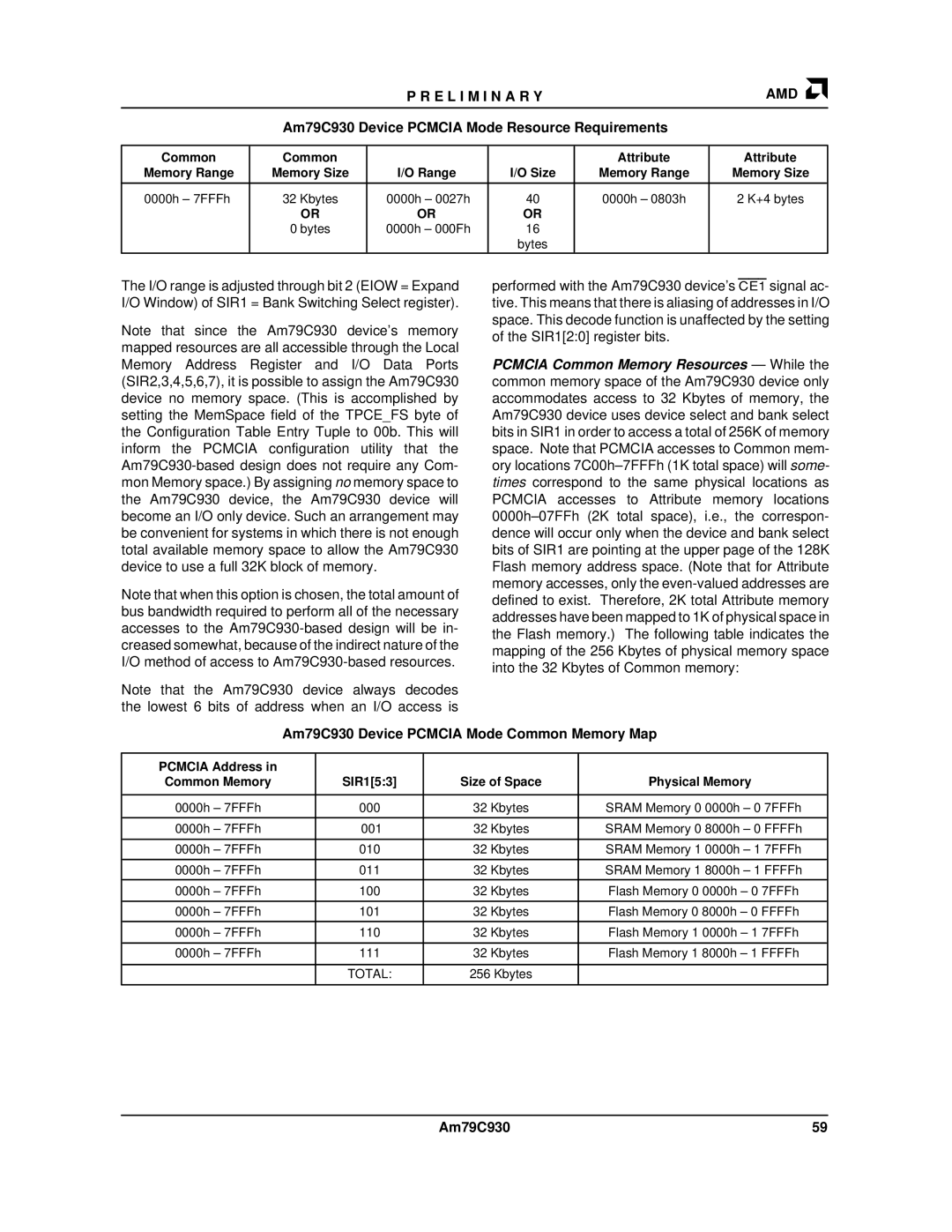
| Am79C930 Device PCMCIA Mode Resource Requirements |
| |||
|
|
|
|
|
|
Common | Common |
|
| Attribute | Attribute |
Memory Range | Memory Size | I/O Range | I/O Size | Memory Range | Memory Size |
|
|
|
|
|
|
0000h – 7FFFh | 32 Kbytes | 0000h – 0027h | 40 | 0000h – 0803h | 2 K+4 bytes |
| OR | OR | OR |
|
|
| 0 bytes | 0000h – 000Fh | 16 |
|
|
|
|
| bytes |
|
|
The I/O range is adjusted through bit 2 (EIOW = Expand I/O Window) of SIR1 = Bank Switching Select register).
Note that since the Am79C930 device's memory mapped resources are all accessible through the Local Memory Address Register and I/O Data Ports (SIR2,3,4,5,6,7), it is possible to assign the Am79C930 device no memory space. (This is accomplished by setting the MemSpace field of the TPCE_FS byte of the Configuration Table Entry Tuple to 00b. This will inform the PCMCIA configuration utility that the
Note that when this option is chosen, the total amount of bus bandwidth required to perform all of the necessary accesses to the
Note that the Am79C930 device always decodes the lowest 6 bits of address when an I/O access is
performed with the Am79C930 device's CE1 signal ac- tive. This means that there is aliasing of addresses in I/O space. This decode function is unaffected by the setting of the SIR1[2:0] register bits.
PCMCIA Common Memory Resources — While the common memory space of the Am79C930 device only accommodates access to 32 Kbytes of memory, the Am79C930 device uses device select and bank select bits in SIR1 in order to access a total of 256K of memory space. Note that PCMCIA accesses to Common mem- ory locations
Am79C930 Device PCMCIA Mode Common Memory Map
PCMCIA Address in |
|
|
|
Common Memory | SIR1[5:3] | Size of Space | Physical Memory |
|
|
|
|
0000h – 7FFFh | 000 | 32 Kbytes | SRAM Memory 0 0000h – 0 7FFFh |
|
|
|
|
0000h – 7FFFh | 001 | 32 Kbytes | SRAM Memory 0 8000h – 0 FFFFh |
|
|
|
|
0000h – 7FFFh | 010 | 32 Kbytes | SRAM Memory 1 0000h – 1 7FFFh |
|
|
|
|
0000h – 7FFFh | 011 | 32 Kbytes | SRAM Memory 1 8000h – 1 FFFFh |
0000h – 7FFFh | 100 | 32 Kbytes | Flash Memory 0 0000h – 0 7FFFh |
|
|
|
|
0000h – 7FFFh | 101 | 32 Kbytes | Flash Memory 0 8000h – 0 FFFFh |
|
|
|
|
0000h – 7FFFh | 110 | 32 Kbytes | Flash Memory 1 0000h – 1 7FFFh |
|
|
|
|
0000h – 7FFFh | 111 | 32 Kbytes | Flash Memory 1 8000h – 1 FFFFh |
|
|
|
|
| TOTAL: | 256 Kbytes |
|
|
|
|
|
Am79C930 | 59 |