P R E L I M I N A R Y | AMD |
|
|
MIR8: Flash Wait States
This register gives the Flash Wait states.
Bit | Name | Reset Value |
| Description |
|
|
|
|
|
|
|
|
|
|
|
7:4 | Reserved | – | Reserved. Must be written as a 0. Reads of this bit produce | ||||
|
|
|
| undefined data. |
|
|
|
3 | HOSTALLOW | 1 |
| When this bit equals 1, then the host can access memory; if 0, then | |||
|
|
|
| the host access is blocked completely | |||
2 | Reserved | – | Reserved. Must be written as a 0. Reads of this bit produce | ||||
|
|
|
| undefined data. |
|
|
|
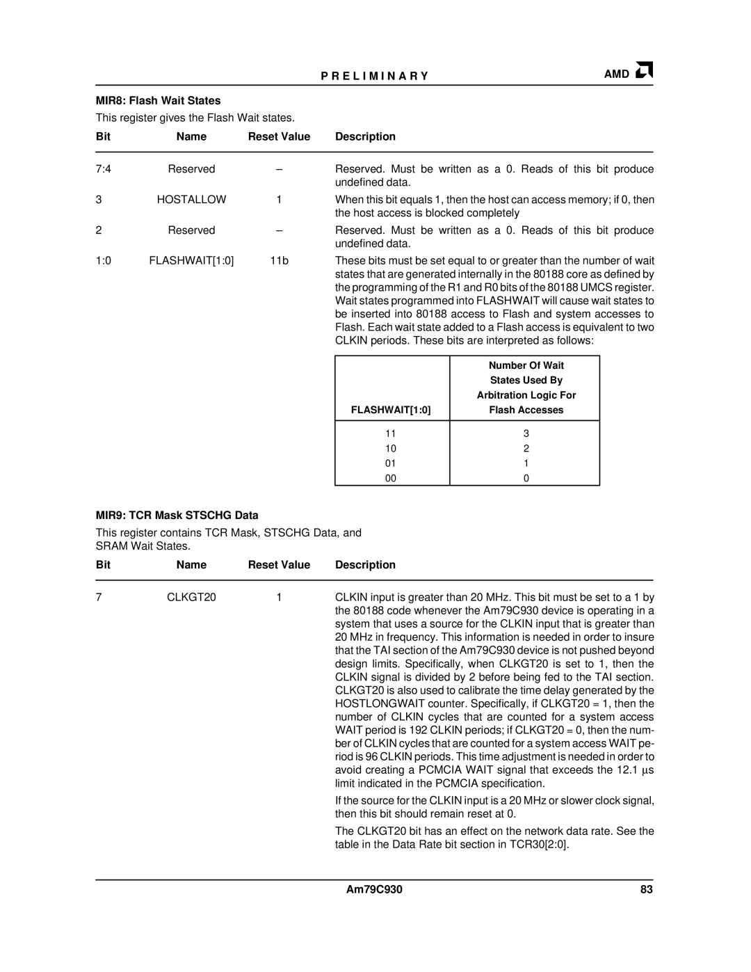
1:0 | FLASHWAIT[1:0] | 11b |
| These bits must be set equal to or greater than the number of wait | |||
|
|
|
| states that are generated internally in the 80188 core as defined by | |||
|
|
|
| the programming of the R1 and R0 bits of the 80188 UMCS register. | |||
|
|
|
| Wait states programmed into FLASHWAIT will cause wait states to | |||
|
|
|
| be inserted into 80188 access to Flash and system accesses to | |||
|
|
|
| Flash. Each wait state added to a Flash access is equivalent to two | |||
|
|
|
| CLKIN periods. These bits are interpreted as follows: | |||
|
|
|
|
|
|
| |
|
|
|
|
| Number Of Wait |
|
|
|
|
|
|
| States Used By |
| |
|
|
|
|
| Arbitration Logic For |
| |
|
|
|
| FLASHWAIT[1:0] | Flash Accesses |
| |
|
|
|
|
|
|
|
|
|
|
|
| 11 | 3 |
|
|
|
|
|
| 10 | 2 |
|
|
|
|
|
| 01 | 1 |
|
|
|
|
|
| 00 | 0 |
|
|
MIR9: TCR Mask STSCHG Data
This register contains TCR Mask, STSCHG Data, and
SRAM Wait States.
Bit | Name | Reset Value | Description |
|
|
|
|
|
|
| |
7 | CLKGT20 | 1 | CLKIN input is greater than 20 MHz. This bit must be set to a 1 by | ||
|
|
| the 80188 code whenever the Am79C930 device is operating in a | ||
|
|
| system that uses a source for the CLKIN input that is greater than | ||
|
|
| 20 MHz in frequency. This information is needed in order to insure | ||
|
|
| that the TAI section of the Am79C930 device is not pushed beyond | ||
|
|
| design limits. Specifically, when CLKGT20 is set to 1, then the | ||
|
|
| CLKIN signal is divided by 2 before being fed to the TAI section. | ||
|
|
| CLKGT20 is also used to calibrate the time delay generated by the | ||
|
|
| HOSTLONGWAIT counter. Specifically, if CLKGT20 = 1, then the | ||
|
|
| number of CLKIN cycles that are counted for a system access | ||
|
|
| WAIT period is 192 CLKIN periods; if CLKGT20 = 0, then the num- | ||
|
|
| ber of CLKIN cycles that are counted for a system access WAIT pe- | ||
|
|
| riod is 96 CLKIN periods. This time adjustment is needed in order to | ||
|
|
| avoid creating a PCMCIA WAIT signal that exceeds the 12.1 μs | ||
|
|
| limit indicated in the PCMCIA specification. |
|
|
|
|
| If the source for the CLKIN input is a 20 MHz or slower clock signal, | ||
|
|
| then this bit should remain reset at 0. |
|
|
|
|
| The CLKGT20 bit has an effect on the network data rate. See the | ||
|
|
| table in the Data Rate bit section in TCR30[2:0]. |
|
|
|
|
|
|
|
|
|
|
| Am79C930 | 83 | |