P R E L I M I N A R Y | AMD |
|
|
2:0 | DR[2:0] | 001b |
TCR31: Device Revision
This register is the Device Revision register.
CONFIGURATION REGISTER INDEX:
Bit | Name | Reset Value |
then a
The control of the function of the TXC pin is described in the Multi- Function Pin section.
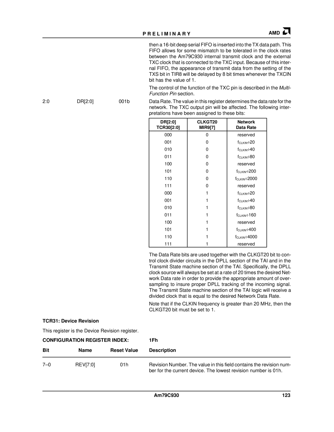
Data Rate. The value in this register determines the data rate for the network. The TXC output pin will be affected. The following inter- pretations have been assigned to these bits:
DR[2:0] | CLKGT20 | Network |
TCR30[2:0] | MIR9[7] | Data Rate |
|
|
|
000 | 0 | reserved |
001 | 0 | fCLKIN÷20 |
010 | 0 | fCLKIN÷40 |
011 | 0 | fCLKIN÷80 |
100 | 0 | reserved |
101 | 0 | fCLKIN÷200 |
110 | 0 | fCLKIN÷2000 |
111 | 0 | reserved |
000 | 1 | fCLKIN÷20 |
001 | 1 | fCLKIN÷40 |
010 | 1 | fCLKIN÷80 |
011 | 1 | fCLKIN÷160 |
100 | 1 | reserved |
101 | 1 | fCLKIN÷400 |
110 | 1 | fCLKIN÷4000 |
111 | 1 | reserved |
The Data Rate bits are used together with the CLKGT20 bit to con- trol clock divider circuits in the DPLL section of the TAI and in the Transmit State machine section of the TAI. Specifically, the DPLL clock source will always be set at a rate of 20 times the desired Net- work Data rate in order to provide the appropriate amount of over- sampling to insure proper DPLL tracking of the incoming signal. The Transmit State machine section of the TAI logic will receive a divided clock that is equal to the desired Network Data Rate.
Note that if the CLKIN frequency is greater than 20 MHz, then the CLKGT20 bit must be set to 1.
1Fh
Description
REV[7:0] | 01h | Revision Number. The value in this field contains the revision num- | ||
|
|
| ber for the current device. The lowest revision number is 01h. | |
|
|
|
|
|
|
|
| Am79C930 | 123 |