P R E L I M I N A R Y | AMD |
|
|
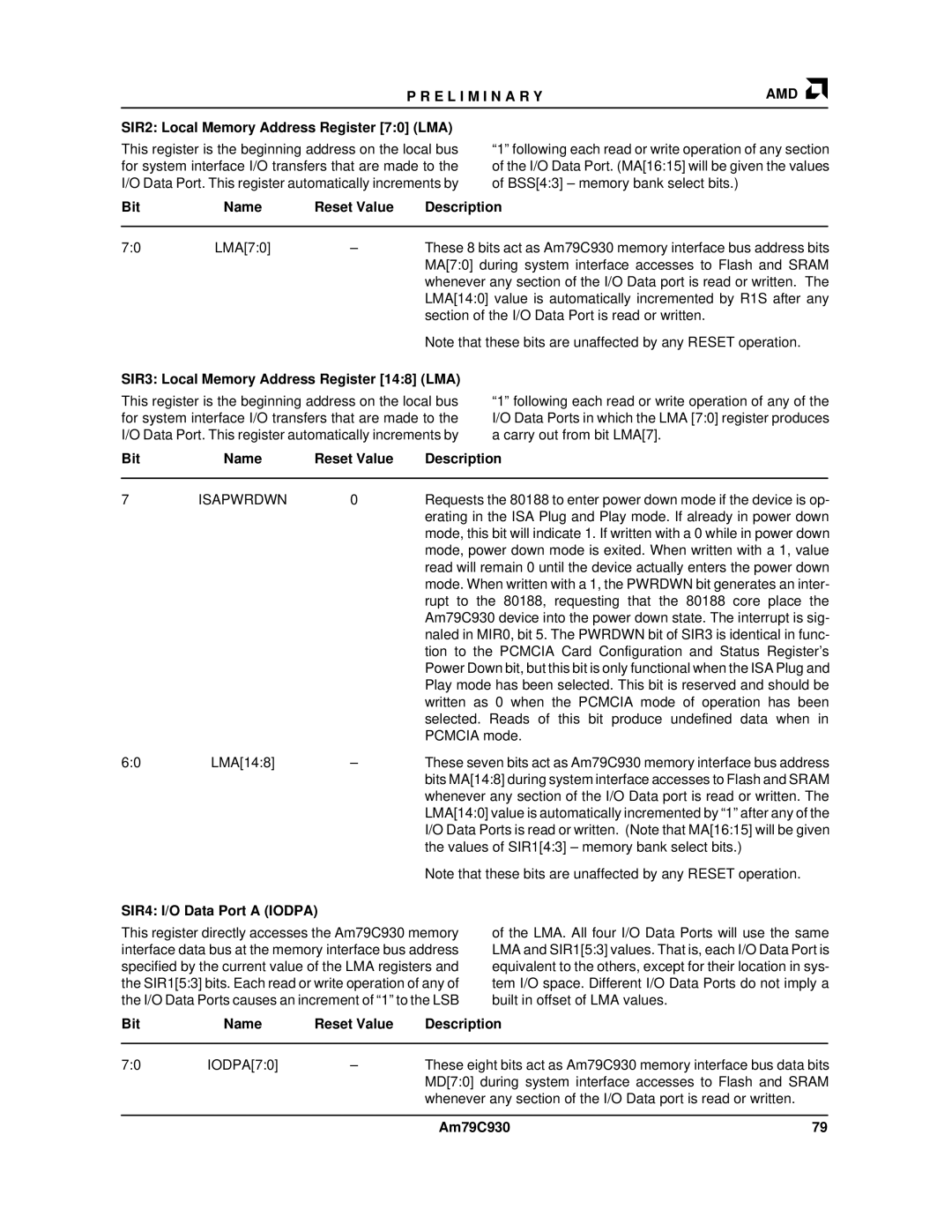
SIR2: Local Memory Address Register [7:0] (LMA)
This register is the beginning address on the local bus for system interface I/O transfers that are made to the I/O Data Port. This register automatically increments by
“1” following each read or write operation of any section of the I/O Data Port. (MA[16:15] will be given the values of BSS[4:3] – memory bank select bits.)
Bit | Name | Reset Value | Description |
|
|
|
|
7:0 | LMA[7:0] | – | These 8 bits act as Am79C930 memory interface bus address bits |
|
|
| MA[7:0] during system interface accesses to Flash and SRAM |
|
|
| whenever any section of the I/O Data port is read or written. The |
|
|
| LMA[14:0] value is automatically incremented by R1S after any |
|
|
| section of the I/O Data Port is read or written. |
|
|
| Note that these bits are unaffected by any RESET operation. |
SIR3: Local Memory Address Register [14:8] (LMA)
This register is the beginning address on the local bus for system interface I/O transfers that are made to the I/O Data Port. This register automatically increments by
“1” following each read or write operation of any of the I/O Data Ports in which the LMA [7:0] register produces a carry out from bit LMA[7].
Bit | Name | Reset Value | Description | |
|
|
|
|
|
7 | ISAPWRDWN | 0 | Requests the 80188 to enter power down mode if the device is op- | |
|
|
| erating in the ISA Plug and Play mode. If already in power down | |
|
|
| mode, this bit will indicate 1. If written with a 0 while in power down | |
|
|
| mode, power down mode is exited. When written with a 1, value | |
|
|
| read will remain 0 until the device actually enters the power down | |
|
|
| mode. When written with a 1, the PWRDWN bit generates an inter- | |
|
|
| rupt to the 80188, requesting that the 80188 core place the | |
|
|
| Am79C930 device into the power down state. The interrupt is sig- | |
|
|
| naled in MIR0, bit 5. The PWRDWN bit of SIR3 is identical in func- | |
|
|
| tion to the PCMCIA Card Configuration and Status Register's | |
|
|
| Power Down bit, but this bit is only functional when the ISA Plug and | |
|
|
| Play mode has been selected. This bit is reserved and should be | |
|
|
| written as 0 when the PCMCIA mode of operation has been | |
|
|
| selected. Reads of this bit produce undefined data when in | |
|
|
| PCMCIA mode. | |
6:0 | LMA[14:8] | – | These seven bits act as Am79C930 memory interface bus address | |
|
|
| bits MA[14:8] during system interface accesses to Flash and SRAM | |
|
|
| whenever any section of the I/O Data port is read or written. The | |
|
|
| LMA[14:0] value is automatically incremented by “1” after any of the | |
I/O Data Ports is read or written. (Note that MA[16:15] will be given the values of SIR1[4:3] – memory bank select bits.)
Note that these bits are unaffected by any RESET operation.
SIR4: I/O Data Port A (IODPA)
This register directly accesses the Am79C930 memory interface data bus at the memory interface bus address specified by the current value of the LMA registers and the SIR1[5:3] bits. Each read or write operation of any of the I/O Data Ports causes an increment of “1” to the LSB
of the LMA. All four I/O Data Ports will use the same LMA and SIR1[5:3] values. That is, each I/O Data Port is equivalent to the others, except for their location in sys- tem I/O space. Different I/O Data Ports do not imply a built in offset of LMA values.
Bit | Name | Reset Value | Description |
|
|
|
|
| |
7:0 | IODPA[7:0] | – | These eight bits act as Am79C930 memory interface bus data bits | |
|
|
| MD[7:0] during system interface accesses to Flash and SRAM | |
|
|
| whenever any section of the I/O Data port is read or written. |
|
|
|
|
|
|
|
|
| Am79C930 | 79 |
