P R E L I M I N A R Y | AMD |
|
|
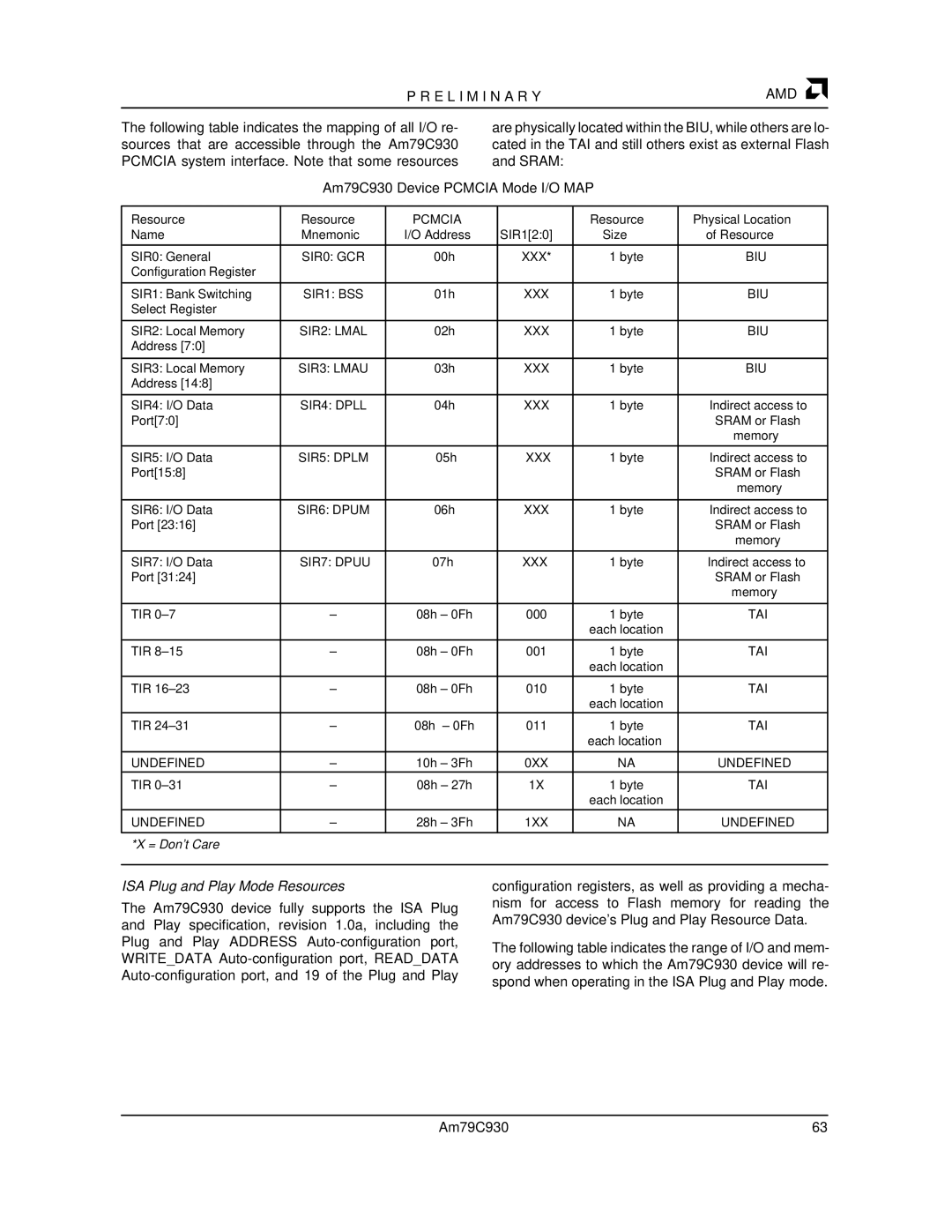
The following table indicates the mapping of all I/O re- sources that are accessible through the Am79C930 PCMCIA system interface. Note that some resources
are physically located within the BIU, while others are lo- cated in the TAI and still others exist as external Flash and SRAM:
Am79C930 Device PCMCIA Mode I/O MAP
Resource | Resource | PCMCIA |
| Resource | Physical Location |
Name | Mnemonic | I/O Address | SIR1[2:0] | Size | of Resource |
|
|
|
|
|
|
SIR0: General | SIR0: GCR | 00h | XXX* | 1 byte | BIU |
Configuration Register |
|
|
|
|
|
|
|
|
|
|
|
SIR1: Bank Switching | SIR1: BSS | 01h | XXX | 1 byte | BIU |
Select Register |
|
|
|
|
|
|
|
|
|
|
|
SIR2: Local Memory | SIR2: LMAL | 02h | XXX | 1 byte | BIU |
Address [7:0] |
|
|
|
|
|
|
|
|
|
|
|
SIR3: Local Memory | SIR3: LMAU | 03h | XXX | 1 byte | BIU |
Address [14:8] |
|
|
|
|
|
|
|
|
|
|
|
SIR4: I/O Data | SIR4: DPLL | 04h | XXX | 1 byte | Indirect access to |
Port[7:0] |
|
|
|
| SRAM or Flash |
|
|
|
|
| memory |
|
|
|
|
|
|
SIR5: I/O Data | SIR5: DPLM | 05h | XXX | 1 byte | Indirect access to |
Port[15:8] |
|
|
|
| SRAM or Flash |
|
|
|
|
| memory |
|
|
|
|
|
|
SIR6: I/O Data | SIR6: DPUM | 06h | XXX | 1 byte | Indirect access to |
Port [23:16] |
|
|
|
| SRAM or Flash |
|
|
|
|
| memory |
|
|
|
|
|
|
SIR7: I/O Data | SIR7: DPUU | 07h | XXX | 1 byte | Indirect access to |
Port [31:24] |
|
|
|
| SRAM or Flash |
|
|
|
|
| memory |
|
|
|
|
|
|
TIR | – | 08h – 0Fh | 000 | 1 byte | TAI |
|
|
|
| each location |
|
|
|
|
|
|
|
TIR | – | 08h – 0Fh | 001 | 1 byte | TAI |
|
|
|
| each location |
|
|
|
|
|
|
|
TIR | – | 08h – 0Fh | 010 | 1 byte | TAI |
|
|
|
| each location |
|
TIR | – | 08h – 0Fh | 011 | 1 byte | TAI |
|
|
|
| each location |
|
|
|
|
|
|
|
UNDEFINED | – | 10h – 3Fh | 0XX | NA | UNDEFINED |
TIR | – | 08h – 27h | 1X | 1 byte | TAI |
|
|
|
| each location |
|
UNDEFINED | – | 28h – 3Fh | 1XX | NA | UNDEFINED |
|
|
|
|
|
|
*X = Don't Care |
|
|
|
|
|
|
|
|
|
|
|
ISA Plug and Play Mode Resources
The Am79C930 device fully supports the ISA Plug and Play specification, revision 1.0a, including the Plug and Play ADDRESS
configuration registers, as well as providing a mecha- nism for access to Flash memory for reading the Am79C930 device's Plug and Play Resource Data.
The following table indicates the range of I/O and mem- ory addresses to which the Am79C930 device will re- spond when operating in the ISA Plug and Play mode.
Am79C930 | 63 |