AMD | P R E L I M I N A R Y |
|
|
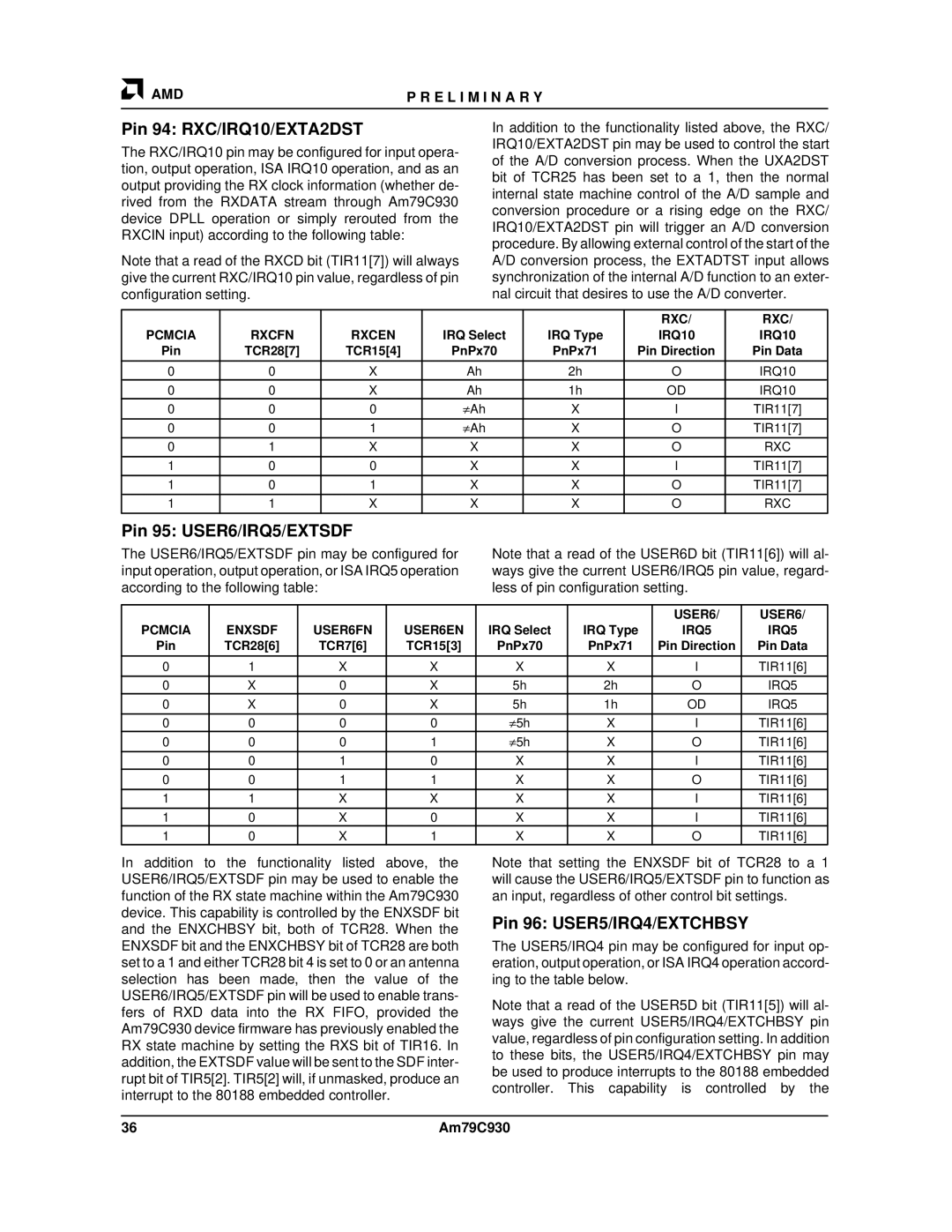
Pin 94: RXC/IRQ10/EXTA2DST
The RXC/IRQ10 pin may be configured for input opera- tion, output operation, ISA IRQ10 operation, and as an output providing the RX clock information (whether de- rived from the RXDATA stream through Am79C930 device DPLL operation or simply rerouted from the RXCIN input) according to the following table:
Note that a read of the RXCD bit (TIR11[7]) will always give the current RXC/IRQ10 pin value, regardless of pin configuration setting.
In addition to the functionality listed above, the RXC/ IRQ10/EXTA2DST pin may be used to control the start of the A/D conversion process. When the UXA2DST bit of TCR25 has been set to a 1, then the normal internal state machine control of the A/D sample and conversion procedure or a rising edge on the RXC/ IRQ10/EXTA2DST pin will trigger an A/D conversion procedure. By allowing external control of the start of the A/D conversion process, the EXTADTST input allows synchronization of the internal A/D function to an exter- nal circuit that desires to use the A/D converter.
|
|
|
|
| RXC/ | RXC/ |
PCMCIA | RXCFN | RXCEN | IRQ Select | IRQ Type | IRQ10 | IRQ10 |
Pin | TCR28[7] | TCR15[4] | PnPx70 | PnPx71 | Pin Direction | Pin Data |
|
|
|
|
|
|
|
0 | 0 | X | Ah | 2h | O | IRQ10 |
0 | 0 | X | Ah | 1h | OD | IRQ10 |
0 | 0 | 0 | ≠Ah | X | I | TIR11[7] |
|
|
|
|
|
|
|
0 | 0 | 1 | ≠Ah | X | O | TIR11[7] |
|
|
|
|
|
|
|
0 | 1 | X | X | X | O | RXC |
|
|
|
|
|
|
|
1 | 0 | 0 | X | X | I | TIR11[7] |
|
|
|
|
|
|
|
1 | 0 | 1 | X | X | O | TIR11[7] |
|
|
|
|
|
|
|
1 | 1 | X | X | X | O | RXC |
Pin 95: USER6/IRQ5/EXTSDF
The USER6/IRQ5/EXTSDF pin may be configured for input operation, output operation, or ISA IRQ5 operation according to the following table:
Note that a read of the USER6D bit (TIR11[6]) will al- ways give the current USER6/IRQ5 pin value, regard- less of pin configuration setting.
|
|
|
|
|
| USER6/ | USER6/ |
PCMCIA | ENXSDF | USER6FN | USER6EN | IRQ Select | IRQ Type | IRQ5 | IRQ5 |
Pin | TCR28[6] | TCR7[6] | TCR15[3] | PnPx70 | PnPx71 | Pin Direction | Pin Data |
|
|
|
|
|
|
|
|
0 | 1 | X | X | X | X | I | TIR11[6] |
|
|
|
|
|
|
|
|
0 | X | 0 | X | 5h | 2h | O | IRQ5 |
0 | X | 0 | X | 5h | 1h | OD | IRQ5 |
0 | 0 | 0 | 0 | ≠5h | X | I | TIR11[6] |
0 | 0 | 0 | 1 | ≠5h | X | O | TIR11[6] |
|
|
|
|
|
|
|
|
0 | 0 | 1 | 0 | X | X | I | TIR11[6] |
0 | 0 | 1 | 1 | X | X | O | TIR11[6] |
|
|
|
|
|
|
|
|
1 | 1 | X | X | X | X | I | TIR11[6] |
|
|
|
|
|
|
|
|
1 | 0 | X | 0 | X | X | I | TIR11[6] |
1 | 0 | X | 1 | X | X | O | TIR11[6] |
In addition to the functionality listed above, the USER6/IRQ5/EXTSDF pin may be used to enable the function of the RX state machine within the Am79C930 device. This capability is controlled by the ENXSDF bit and the ENXCHBSY bit, both of TCR28. When the ENXSDF bit and the ENXCHBSY bit of TCR28 are both set to a 1 and either TCR28 bit 4 is set to 0 or an antenna selection has been made, then the value of the USER6/IRQ5/EXTSDF pin will be used to enable trans- fers of RXD data into the RX FIFO, provided the Am79C930 device firmware has previously enabled the RX state machine by setting the RXS bit of TIR16. In addition, the EXTSDF value will be sent to the SDF inter- rupt bit of TIR5[2]. TIR5[2] will, if unmasked, produce an interrupt to the 80188 embedded controller.
Note that setting the ENXSDF bit of TCR28 to a 1 will cause the USER6/IRQ5/EXTSDF pin to function as an input, regardless of other control bit settings.
Pin 96: USER5/IRQ4/EXTCHBSY
The USER5/IRQ4 pin may be configured for input op- eration, output operation, or ISA IRQ4 operation accord- ing to the table below.
Note that a read of the USER5D bit (TIR11[5]) will al- ways give the current USER5/IRQ4/EXTCHBSY pin value, regardless of pin configuration setting. In addition to these bits, the USER5/IRQ4/EXTCHBSY pin may be used to produce interrupts to the 80188 embedded controller. This capability is controlled by the
36 | Am79C930 |