Chapter 4 Digital Modules | SMART I/O User’s Manual | |||
|
|
|
|
|
|
|
|
|
|
4.2.5 Functional Description
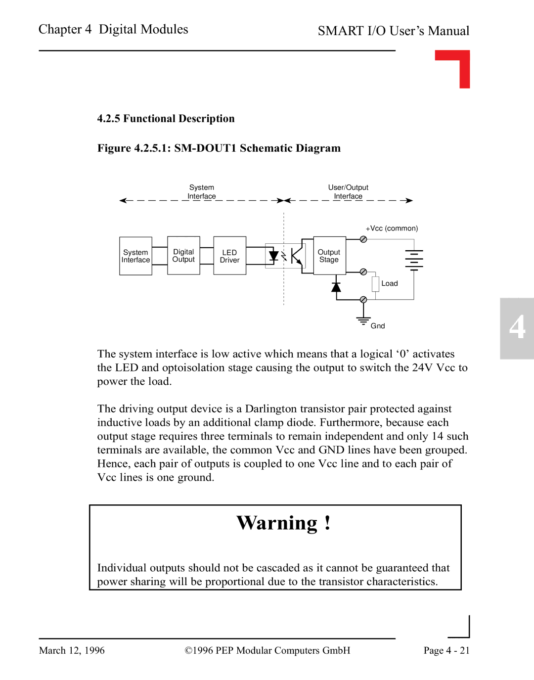
Figure 4.2.5.1: SM-DOUT1 Schematic Diagram
System | User/Output |
Interface | Interface |
System
Interface
Digital Output
LED
Driver
+Vcc (common)
Output
Stage
Load
|
|
|
|
|
|
|
|
|
|
| 4 |
|
|
|
|
|
|
|
| Gnd | |||
|
|
|
|
|
|
|
| ||||
|
|
|
|
|
|
|
|
| |||
The system interface is low active which means that a logical ‘0’ activates the LED and optoisolation stage causing the output to switch the 24V Vcc to power the load.
The driving output device is a Darlington transistor pair protected against inductive loads by an additional clamp diode. Furthermore, because each output stage requires three terminals to remain independent and only 14 such terminals are available, the common Vcc and GND lines have been grouped. Hence, each pair of outputs is coupled to one Vcc line and to each pair of Vcc lines is one ground.
Warning !
Individual outputs should not be cascaded as it cannot be guaranteed that power sharing will be proportional due to the transistor characteristics.
|
|
|
|
March 12, 1996 | ©1996 PEP Modular Computers GmbH | Page 4 - 21 | |
|
| ||