TX39 Family Core Architecture
Page
Toshiba
Contents
EPC Exception Program Counter register
Memory location of exception vectors
Appendix a Instruction Set Details
Coprocessor Unusable exception
Bus Interface Unit Bus Controller / Write Buffer
229
227
Bus request and bus grant 227 Cache snoop 228
230
Architecture
Architecture
Introduction
Features
High-performance Risc techniques
Low power consumption
Mathematical notation
Signal notation
Notation Used in This Manual
Data notation
Architecture
Architecture
Overview
Registers
CPU registers
CP0 registers
Reserved †
Exception program counter
Source register 5 bits
Instruction Set Overview
Operation code 6 bits
Destination register 5 bits
Jump/branch
Load/store
Computational
Coprocessor
ALU Immediate
Computational Instructions
ALU 3-operand, register type
Coprocessor Instructions
Multiply/Divide
Jump/Branch Instructions
Special Instructions
Special Instruction
CP0 instructions Instruction Description CP0 Instructions
Data Formats and Addressing
Big endian and little endian formats
Architecture
Byte addresses of a misaligned word
Pipeline Processing Overview
Memory Management Unit MMU
User mode
Kernel mode
1 R3900 Processor Core operating modes
Kseg0
Direct segment mapping
Kuseg
Kseg1
Address mapping
Architecture
Instruction Formats
Instruction Set Overview
Instruction Notation
Byte specifications for load and store instructions
Load and Store Instructions
Base Offset
Sync
Computational Instructions
NOR
SLLV, SRLV, Srav Instruction Format and Description
MFHI, Mflo Instruction Format and Description
MTHI, Mtlo Instruction Format and Description
Architecture
Jump instructions
Jump/Branch Instructions
Instruction Format and Description
Instruction in the delay slot is executed during the jump
10. Branch instructions
Architecture
Special Instructions
11. Special instructions
COPz Instruction Format and Description
Coprocessor Instructions
BCzT, BCzF Instruction Format and Description
Architecture
13. System control coprocessor CP0 instructions
Restore From
System Control Coprocessor CP0 Instructions
Cache Instruction Format and Description
Pipeline Architecture
Delayed load
Delay Slot
Delayed branching
Nonblocking Load Function
Nonblocking load function
Divide Instruction DIV, Divu
Streaming
Memory Management Unit MMU
R3900 Processor Core Operating Modes
Direct Segment Mapping
Internal MMU virtual address space
Kuseg
512MB
Exception Processing
Utlb
TLBL2
Status register
Exception Processing Registers
Cause register
Cache register
Bits Mnemonic Field name Description
Cause register register no.13
Read/Write
ExcCode field
Mnemonic Cause
Field name Description
Status register register no.12
Bits
Read
Status register 1/2
Bits Mnemonic Field name Description Value on Read
NmI Non-maskable Interrupt
KUc/KUp/KUo Kernel/User mode current/previous/old
IEc/IEp/IEo Interrupt Enable current/previous/old
IntMask Interrupt Mask
Cache register register no.7
Cache register
DALc/DALp/DALo Data Cache Auto-Lock current/previous/old
IAL DAL
Shows how the RFE instruction works
BadVAddr Bad Virtual Address register register no.8
PRId Processor Revision Identifier register register no.15
Config Configuration register register no.3
21-19
10. Config register2/2
Exception Details
∙ Applicable instructions
Address Error exception ∙ Causes
∙ Exception mask
∙ Processing
Breakpoint exception ∙ Cause
∙ Servicing
Bus Error exception ∙ Causes
Architecture
Coprocessor Unusable exception ∙ Cause
Interrupts ∙ Cause
Overflow exception ∙ Cause
Reserved Instruction exception ∙ Cause
Reset exception ∙ Cause
System Call exception ∙ Cause
Non-maskable interrupt ∙ Cause
Architecture
Return from Exception Handler
Priority of Exceptions
Priority of Exceptions Exception Mnemonic
Architecture
Caches
Instruction Cache
Data cache configuration
Data Cache
Lock function
Lock bit setting
Operation during lock
Lock bit clearing
Auto-lock bits
Cache flushing
Cache Test Function
Cache disabling
Example
Cache Refill
Cache refill
Cache Snoop
Architecture
Debugging Functions
System Control Processor CP0 Registers
PRId Processor revision ID Debug †† Debug exception control
Depc ††
DM Debug Mode 0 at reset
DBD Debug Branch Delay
Debug register register no.16
NIS Non-maskable Interrupt Status
BsF Bus Error Exception Flag
SSt Single at reset
OES Other Exceptions Status
Types of debug exceptions
Debug Exceptions
DSS bit
Debug Single Step DSS
Branching to a debug exception handler
Ii Debug exception handler execution
Executing a Deret instruction
Iii Return from a debug exception handler
Exception priorities
Single Step exception ∙ Cause
Details of Debug Exceptions
∙ Exception masking
∙ Instruction causing this exception
Debug Breakpoint exception ∙ Cause
Architecture
Appendix a Instruction Set Details
Instruction Classes
Instruction Formats
Instruction Notation Conventions
Twos complement division
Bitwise logical XOR operation
Examples of Instruction Notation
Table A-2. Common Load/Store Functions
Function Meaning
Halfword access 16 bits
Word access 32 bits
Triplebyte access 24 bits
Byte access 8 bits
Jump and Branch Instructions
ADD
Addi
Addiu
Addu
Rd, rs, rt
Andi
BCzF
Operation Code Bit Encoding
BCzFL
111
BCzT
113
BCzTL
115
BEQ
Beql
Bgez
Bgezal
Bgezall
Bgezl
Bgtz
Bgtzl
Blez
Blezl
Bltz
Bltzal
Bltzall
Bltzl
BNE
Bnel
Break
Bit# Cache Name
Data
Bit# Cache Operation Description Name
CFCz
COPz
COPz
CTCz
Deret
DIV
Divu
Jump
JAL
Jalr
JR rs
LB rt, offsetbase
LBU
LH rt, offsetbase
LHU
LUI
LW rt, offsetbase
LWL
152
LWR
154
Multiply/Add
Maddu
MFC0
MFCz
MFCz
MFCz
Mfhi
Mflo
MTC0
MTCz
MTCz
Mthi
Mtlo
Mult
Multu
NOR
Or rd, rs, rt
ORI
RFE
SB rt, offsetbase
Sdbbp
SH rt, offsetbase
SLL
Sllv
SLT
Slti
Sltiu
Sltu
SRA
Srav
SRL
Srlv
SUB
Subu
SW rt, offsetbase
SWL
189
SWR
191
Sync
Syscall
XOR
Xori
Special function
OPcode
COPz rs
COPz rt
CP0 Function
Notation
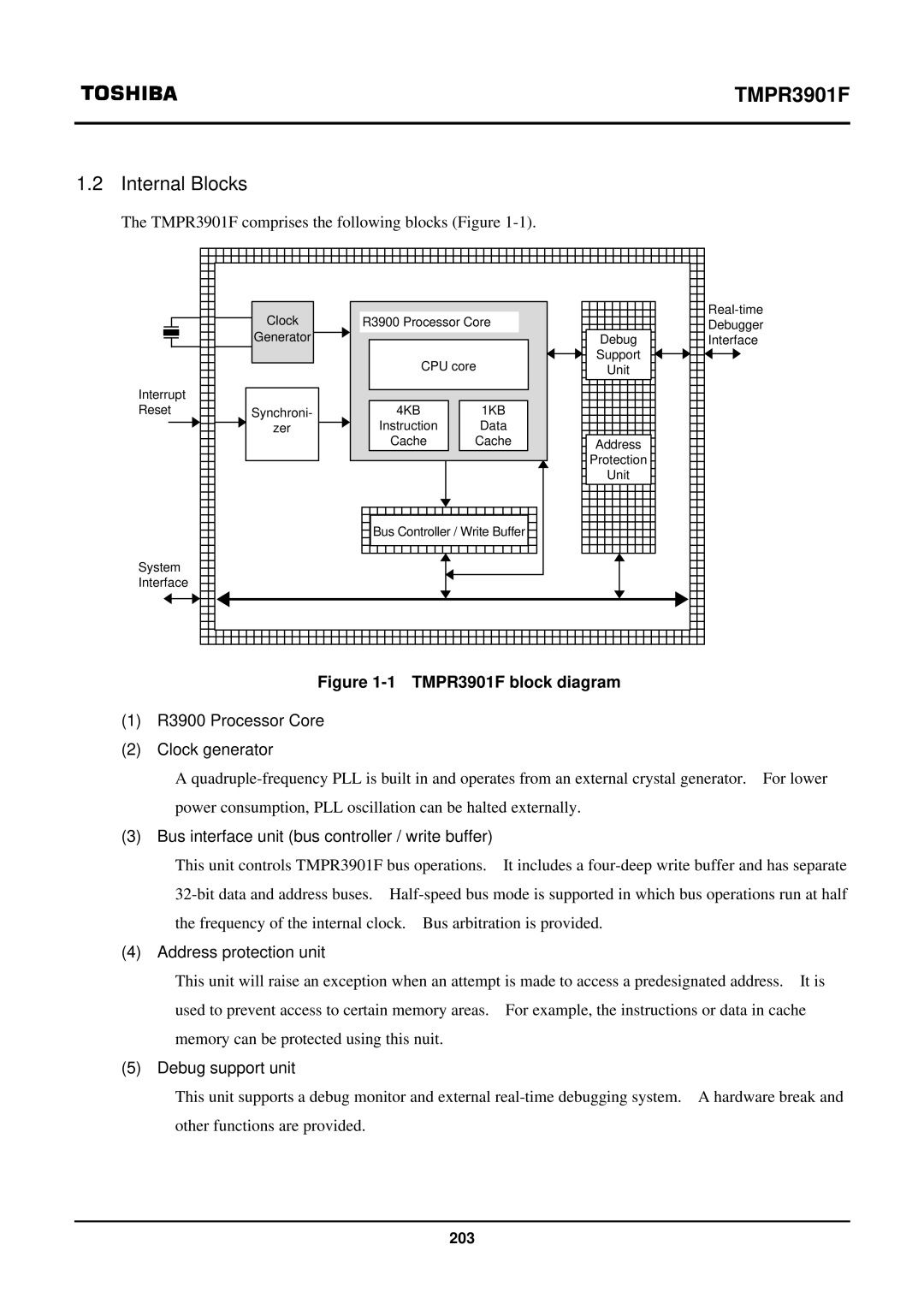
TMPR3901F
200
On-chip peripheral circuits
R3900 Processor Core
Bus interface for ease of system implementation
Maximum operating frequency
Low power consumption, optimal for portable applications
Debugging support functions on chip
Package
Bus interface unit bus controller / write buffer
Internal Blocks
R3900 Processor Core Clock generator
Address protection unit
204
R3900 Processor Core
Configuration
Instruction Iimitations
Clock Generator
Address mapping
Sync NOP
Address Protection Unit
Registers Break Address register BAddr0-1
Break Mask register BMsk0-1
Break Control register BCnt0-1
Break Status register BSts
Memory protection exception
Register address map
Debug Support Unit
Synchronizer
BSts 0xFF00 BAddr0 Bcnt0 BMsk0 BAddr1 Bcnt1 BMsk1
INT* signal synchronization
INT50
NMI* signal synchronization
CPCOND* signal synchronization
CPCOND31
Pins
Halt signal. Indicates that TMPR3901F is in halt mode
Enables internal PLL clock
Mode quadruple frequency of crystal oscillator
Doze signal. Indicates that TMPR3901F is in doze mode
∙ Master Clock
Operations
Clock
∙ Processor Clock
System clock
Master clock Processor
Clock
Read Operation
Single Read
Bus error during a single read operation
Burst Read
Burst read 4 words 1 wait
Bus error in burst read operation 4 words
Write Operation
Single write operation 2 waits
Interrupts
1 NMI
2 INT50
Interrupt
Bus Arbitration
Bus request and bus grant
BUSGNT*L
Reset
Half-Speed Bus Mode
Single read operation in half-speed bus mode
Power-Down Mode
Halt mode
232
Standby Mode
Standby mode PLL stop
Doze Mode
Reduced Frequency Mode