Intel 460GX Chipset System Software Developer’s Manual
Intel 460GX Chipset System Software Developer’s Manual
Contents
Coherency
10.1
Latency
10-1
11-8
13.2.4
Figures
Tables
12-11
System Overview
Introduction
Intel 460GX Chipset Components
Component Overview
Name Function
Itanium Processor System Bus Support
Product Features
Dram Interface Support
PXB Features
I/O Support
GXB Features
RAS Features
Reference Documents
Other Platform Components
1 I/O & Firmware Bridge IFB
Programmable Interrupt Device PID
Date Description June Initial release
Revision History
Introduction
Register Descriptions
Access Mechanism
Partitioning
Access Restrictions
Device Mapping on Bus CBN
Device
Register Attributes
Default Upon Reset
Reserved Bits Defined in Registers
Reserved or Undefined Register Locations
I/O Mapped Registers
Configaddress Configuration Address Register
Consistency
Gart Programming Region
Configdata Configuration Data Register
Error Handling Registers
1 SAC
1.1
1.2
Bits Description Disable
1.3
Valid
Ferrsac First Error Status Register
Nerrsac All Error Status Register
Biuitid BIU Itid Register
Saferr System Address on First Error
Address bits
Biudata BIU Data Register
2.1 SEC0DFERR Data on First Memory Card B SEC
2 SDC
2.2 SEC0ECCFERR ECC on First Memory Card B SEC
2.3 SEC0TXINFOFERR Txinfo on First Memory Card B SEC
2.5 DED0ECCFERR ECC on First Memory Card B DED
2.4 DED0DFERR Data on First Memory Card B DED
2.6 DED0TXINFOFERR Txinfo on First Memory Card B DED
2.7 SEC1DFERR Data on First Memory Card a SEC
2.9 SEC1TXINFOFERR Txinfo on First Memory Card a SEC
2.8 SEC1ECCFERR ECC on First Memory Card a SEC
2.10 DED1DFERR Data on First Memory Card a DED
2.11 DED1ECCFERR ECC on First Memory Card a DED
Sdcferr First Error Status Register
2.12 DED1TXINFOFERR Txinfo on First Memory Card a DED
21 ’Forward’ Underflow Card a Left Stack Error FL1
22 ’Forward’ Underflow Card a Right Stack Error FR1
15 ’Forward’ Underflow Card B Right Stack Error FR0
14 ’Forward’ Underflow Card B Left Stack Error FL0
Pcmdferr Command on First Pcmd Parity Error
Sdcnerr SDC Next Error Status Register
Pitidferr Data on First Pitid Parity Error
Dpbrleferr Private Data Bus Receive Length Error
Sdcrspferr Response on First Sdcrsp Error
ECCMSK0 ECC Mask Register Card B
ECCMSK1 ECC Mask Register Card a
ParMskP PB Parity Mask and IB Correction Enable Register
Eccmskf ECC Mask Register
Pvdparferr Parity on First PVD Parity Error
Pvddferr Data on First PVD Parity Error
Pvdtxinfoferr Txinfo on First PVD Parity Error
Secfeccferr ECC on First System Bus SEC
Secfdferr Data on First System Bus SEC
Secftxinfoferr Txinfo on First System Bus SEC
Dedfdferr Data on First System Bus DED
Que-Overflow Error
Ferrmac First Error Status Register
3 MAC
Dedfeccferr ECC on First System Bus DED
Errsts Error Status Register
Cmndferr Command on First Error
4 PXB
Errcmd Error Command Register
5 GXB
Ferragp First Error Status Register for AGP
5.1
Ferrpci
Nerragp Next Errors Status Register for AGP
Ferrgart First Error Status Register for Gart
Pderr PCI Data First Error
Pacerr PCI Address & Cmd First Error
Nerrgart
Fepci Register Records an PCI Bus Error Flag
Nepci Register Records an PCI Bus Error Flag
6 WXB
Bits Description Intrq Asserted Flag
Fepci PCI Bus First Error Status Register
Nepci PCI Bus Next Error Status Register
Fepcidl PCI First Error Data Log
Fepcial PCI First Error Address/Command Log
Performance Monitor Registers
6764 C/BE30 6332 AD6332 310 AD310
Count Value
Overflow
Length Encodings
Dmask Encodings
Event Select
Umask Encodings
Enable Source
Disable Source
Reload Control
2 SDC
FSBDPMD1,0 System Bus Performance Monitor Data Registers
3.1 PMD10 Performance Monitoring Data Register
3 PXB
3.2 PMR10 Performance Monitoring Response
3.3 PME10 Performance Monitoring Event Selection
Reload Mode
Count Data Cycles
Initiating Agent Selection
AGPPMD0,1 AGP Performance Monitor Data Registers
4 GXB
Percon Performance Monitor Control Register
Pcipmd PCI Performance Monitor Data Registers
Event 1 Input
Event 0 Input
AGPPMC0,1 AGP Performance Monitor Configuration Register
Pipe or Sideband Request Mask
EVENT1 Count Enable
Pcipmc PCI Performance Monitor Configuration Register
Initiating Agent
Disable Source
5 WXB
PCIWXBPMC0 PCI Performance Monitor Configuration Register
Data Transfer and Transaction Qualifier
Issuing Agent Qualifier
Interrupt Related Registers
PCIWXBPMC1 PCI Performance Monitor Configuration Register
Xtprs External Task Priority Registers
PID PCI Memory-mapped Registers
Address Name Access Default Value
2.1 I/O Register Select Register FEC00000h
Memory-Mapped Register Summary
2.2 I/O Window Register FEC00010h
PID Indirect Access Registers
XAPIC EOI Register FEC00040h
I/O Window Register Format
3.1 I/O xAPIC ID Register 00h
Offset Name Access Default Value
RTE
Memory-mapped Register Summary Cont’d
3.3 I/O xAPIC Arbitration ID Register 02h
3.2 I/O xAPIC Version Register 01h
I/O Apic ID Register Format
I/O xAPIC Version Register Format
3.4 I/O xAPIC RTE 10h-8Fh
Bits Sapic Mode Apic Mode Description Name
I/O xAPIC Arbitration ID Register Format
10. I/O xAPIC RTE Format
10. I/O xAPIC RTE Format Cont’d
Sapic Mode Apic Mode Description Name
Vector
Destination
Coherency
System Architecture
Processor Coherency
PCI Coherency
Ordering
AGP Coherency
WXB Arbitration at the PCI Bus
WXB Arbitration
Arbitration for Inbound Transactions
Indivisible Operations
Big-endian Support
Processor Locks
Arbitration for Outbound Transactions
Atomic Writes
Inbound PCI Locks
Atomic Reads
Locks with AGP Non-coherent Traffic
WXB PCI Hot-Plug Support
Interrupt Delivery
Slot Power-down and Disable
Slot Power-up and Enable
System Architecture
Memory Map
System Address Map
Compatibility Region
System Memory Address Space
System Firmware
Medium Extended Memory Region
Low Extended Memory Region
Re-mapped Memory Areas
High Extended Memory above 4G
Variable GAP
Itanium Processor and Chipset-specific Memory Space
I/O Address Map
System I/O Address Space
High PXB must ignore GXB must BINIT# after Gart
Devices View of the System Memory Map
Address Disposition
Legal and Illegal Address Disposition
Address Range Outbound Inbound Dest. Decision
Main memory if present above 4 GB
Address Disposition Cont’d
Above TOM
Binit
System Address Map
Memory Subsystem
General Memory Characteristics
Organization
System
Maximum Memory Configuration Using Two Cards
Technology & Configuration Size
Minimum/Maximum Memory Size per Configuration
Dimm Types
Double Number Memory Size
Address Interleaving
Interleaving/Configurations
Non-uniform Memory Configurations
Summary of Configuration Rules
Bandwidth
Memory Subsystem Clocking
Supporting Features
Auto Detection
Removing a Bad Row
Memory Scrubbing
Hardware Initialization
Scrubbing Time
Memory Size Time to Scrub
Memory Subsystem
Integrity
Data Integrity and Error Handling
System Bus
Expander Buses
Dram
PCI Buses
5 AGP
Memory ECC Routing
Usage of First-error and Next-error
Data Poisoning
BERR#/BINIT# Generation
Masked Bits
INTREQ#
Data ECC or Parity Errors
SAC/SDC Errors
XBINIT#
XSERR#
SAC to SDC Interface Errors
System Bus Errors
5 SDC/Memory Card Interface Errors
SAC to MAC Interface Errors
6 SDC/System Bus Errors
Error Determination
SDC Internal Errors
SAC Address on an Error
Special Notes on Usage of SECTID, DEDTID, Fsetid Registers
SDC Logging Registers
Multiple Errors
Clearing Errors
1 SAC/SDC Error Clearing
ERR ERR
SDC Multiple Errors
Single Errors with Multiple Reporting
SAC Multiple Errors
Error Anomalies
SAC Error Flow on Data
Data Flow Errors
Table of Errors
Error Conditions
SAC to SDC Interface Errors
Error Cases
System Bus ADD/CMND
Error Cases Cont’d
Internal SDC Error
Detected as PCI Master
PXB Errors
PCI Bus Monitoring
PCI Integrity
PXB as Master
Master Abort
PXB as Target
Target Retry
GXB Error Flow
Target Abort
GXB Errors
GXB Error Signals
Gart Interface Errors
GXB Error Flow
Multiple Errors
Usage of First Error and Next Error Registers
WXB Data Integrity and Error Handling
Integrity
Data Parity Poisoning
Error Steering/Signaling
Error Mask Bits
Supported Error Escalation to XBINIT#a
Abbreviation Error
Supported Error Escalation to PA/BINTRQ#
Supported Error Escalation to SERROUT#a
SERR# Generation
Escalation
INTRQ# Interrupt
Error Determination and Logging
XBINIT# Generation
WXB as Bus Master
Error Conditions
Other Violations
WXB as Target
System Error Signaled
PCI Interface Errors
Discard Timer Expiration
Graphics Address Relocation Table Gart
AGP Subsystem
24b
12b
22b
14b
Gart Entry Format for 4kB Pages
Gart Implementation
Sizes
Programming Gart
Gtlb
Parity
SGW#
Coherency
SE2 ADSC# ADSP# ADV# LBO# SB# SW#
AGP Traffic
4.1 3.3V AGP 1X and 2X Mode Compatibility
Interrupt Handling
Addresses Used by the Graphics Card
Coherency, Translation and Types of AGP Traffic
Traffic Priority
Processor Locks and AGP Traffic
Ordering Rules
Coherency for AGP/PCI Streams
Address Alignment and Transfer Sizes
Address Faults
PCI Semantics Traffic
Inbound Reads
PCI Stream Read Prefetching
Inbound Delayed Read Matching Rules
Inbound Reads Directed To Memory
Command Address BEs
Delayed Read Matching Criteria
Inbound I/O Reads
Inbound Writes
Outbound Reads
Retry/Disconnect Conditions
Outbound Writes
Fast Back-to-Back Transactions
Transfer Data Length Combining Supported Used Mode
Burst Write Combining Modes
1st write 2nd write 3rd write Transferred as
GXB Address Map
Latency
Inbound Read Prefetching
Bandwidth Estimates for Various Request Sizes
AGP Subsystem
AGP Subsystem
WXB Hot-Plug
Ihpc Configuration Registers
Ihpc Configuration Register Space
VID Vendor Identification Register
Number List for the Ihpc PCI Register Descriptions
Did Device Identification Register
Pcicmd PCI Command Register
RID Revision Identification Register
Pcists PCI Status Register
Class Class Register
MLT Master Latency Timer Register
CLS Cache Line Size
HDR Header Register
Svid Subsystem Vendor Identification
Base Address
SID Subsystem ID
Interrupt Line
Interrupt Pin
Miscellaneous Hot-Plug Configuration
Hot-Plug Slot Identifier
Switch Change Serr Status
Hot-Plug Features
Power Fault Serr Status
Memory Mapped Register Access Port
Memory Access Index
Ihpc Memory Mapped Registers
Arbiter Serr Status
M66EN
Ihpc Memor Mapped Register Space
Number List for Ihpc Memory Mapped Register Descriptions
Slot Enable
LED Control
Hot-Plug Miscellaneous
Hot-Plug Interrupt Input and Clear
Hot-Plug Interrupt Mask
Serial Input Byte Data
General Purpose Output
Serial Input Byte Pointer
Hot-Plug Non-interrupt Inputs
Slot Power Control
Hot-Plug Switch Interrupt Redirect Enable
Extended Hot-Plug Miscellaneous
PCI Configuration Registers Function
PCI / LPC / FWH Configuration
Mnemonic Register Register Access
IFB Register Mapping
Pcists
Biosen
Classc
Hedt
PCI Configuration Registers-Function 1 IDE Interface
IDE Configuration
PCI Configuration Registers-Function 2 USB Interface
Universal Serial Bus USB Configuration
Configuration Offset Mnemonic Register
SMBus Configuration Registers Function
SMBus Controller Configuration
IFB Register Mapping
Usage of the SW SMI# Timer
Usage of 1MIN Timer in Power Management
CD-ROM Auto RUN Feature of the OS
IFB Usage Considerations
Reserved Secondary Primary Drive Ultra DMA Mode Enable
Ultra DMA Configuration
Disabled Enabled
SSDE1 SSDE0 PSDE1 PSDE0
Overview
Determining a Drive’s Transfer Rate Capabilities
Capability Word Bits Field Offset
Ultra DMA Fields that Indicate Ultra DMA Drive Capabilities
DMA
Capability Word Bits
PIO
Capability Word Bits Field
Determining a Drive’s Best Ultra DMA Capability
150 Minimum Multi Word DMA Transfer Cycle Time per
Capability Word Offset Bits Field
10-6
Determining a Drive’s Best PIO Capability
Drives Reported DMA Drive’s Best DMA Mode Cycle Time
Drive PIO Capability as a Function of Cycle Time
Drives Reported PIO Drive’s Best PIO Mode
10.5.6.1 DMA/PIO Timing Settings
IFB Timing Settings
IFB Drive Mode Based on DMA/PIO Capabilities
Mode Yes Disabled Enabled DMA Mode Iordy If fixed disk
DMA Iordy IDE
Ultra DMA Timing Settings
Drive Configuration for Selected Timings
10. Ultra DMA Timing Value Based on Drive Mode
DMA/PIO Timing Values Based on Piix Cable Mode/System Speed
Drive’s Selected PIO Speed Capability
12. PIO Transfer/Mode Values
10-12
13. Drive Capabilities Checklist
Settings Checklist
Example #1 Ultra DMA/33 Configuration
Example Configurations
14. IFB Settings Checklist
Register Type Offset Value Comments
40-41h E377h Mode config. for Primary IDE Timing Register
Example #3 Non Ultra DMA/33 Drive Configuration
4A-4Bh 0002h Ultra DMA mode config
44h 0Bh Ultra DMA Control Register
4A-4Bh 0000h
Ultra DMA System Software Considerations
10-16
Intel 460GX Chipset Software Developer’s Manual 10-17
BMISX-Bus Master IDE Status Register I/O
Bit Description Reserved. This bit is hardwired to
Bit Description
Completed or halted
Bit Type Description
USB Resume Enable Bit
10-20
VID-Vendor Identification Register Function
LPC/FWH Interface Configuration
DID-Device Identification Register Function
PCISTS-PCI Device Status Register Function
PCICMD-PCI Command Register Function
CLASSC-Class Code Register Function
RID-Revision Identification Register Function
HEDT-Header Type Register Function
Bit
Acpi Base Address Function
Acpi Enable Function
SCI IRQ Routing Control
PIRQRCAD-PIRQx Route Control Registers Function
BIOSEN-BIOS Enable Register Function
TOM-Top of Memory Register Function
SerIRQC-Serial IRQ Control Register Function
Deterministic Latency Control Register Function
MSTAT-Miscellaneous Status Register Function
MGPIOC-Muxed Gpio Control Function
PDMACFG-PCI DMA Configuration Resister Function O
Bits Description
Base Offset Channel
RTCCFG-Real Time Clock Configuration Register Function
Gpio Base Address Function
Gpio Enable Function
LPC COM Decode Ranges Function
Bits Decode Range
000
LPC FDD/LPT Decode Ranges Function
011
110
LPC Generic Decode Range Function
LPC Sound Decode Ranges Function
220 233 240 253 260 273 280 293
11-12
Firmware Hub FWH Decode Enable Register
LPC Enables Function
Reserved. This bit must be a
1413 Reserved
Firmware Hub FWH Select Register
Dcom-Dma Command Register I/O
Test Mode Register
PCI to LPC I/O Space Registers
DMA Registers
Dr-Dma Request Register I/O
Dcm-Dma Channel Mode Register I/O
RWAMB-Read / Write All Mask Bits I/O
WSMB-Write Single Mask Bit I/O
Bit Description Reserved. Must be
DBADDR-DMA Base and Current Address Registers I/O
Ds-Dma Status Register I/O
DBCNT-Dma Base and Current Count Registers I/O
When counting down a DMA transfer
DLPAGE-DMA Low Page Registers I/O
DCBP-Dma Clear Byte Pointer Register I/O
Interrupt Controller Registers
11.2.2.1 Icw1-Initialization Command Word 1 Register I/O
Dmc-Dma Master Clear Register I/O
Dclm-Dma Clear Mask Register I/O
11.2.2.3 Icw3-Initialization Command Word 3 Register I/O
11.2.2.2 Icw2-Initialization Command Word 2 Register I/O
Bit Description Reserved. Must be programmed to all 0s
11.2.2.5 Icw4-Initialization Command Word 4 Register I/O
11.2.2.4 Icw3-Initialization Command Word 3 Register I/O
11.2.2.6 Ocw1-Operational Control Word 1 Register I/O
11-22
11.2.2.8 Ocw3-Operational Control Word 3 Register I/O
11.2.2.7 Ocw2-Operational Control Word 2 Register I/O
Elcr1-Edge/Level Control Register I/O
Tcw-Timer Control Word Register I/O
Counter/Timer Registers
Elcr2-Edge/Level Control Register I/O
Bit Decription
5. When bit 3=0, status and/or count will not be latched
Latched. When bit 4=1, the status will not be latched
5. When bit 2=0, status and/or count will not be latched
5. When bit 1=0, status and/or count will not be latched
TMRCNT-Timer Count Registers I/O
TMRSTS-Timer Status Registers I/O
Nmisc-Nmi Status and Control Register I/O
NMI Registers
Real Time Clock Registers
NMI Enable. Used by IFB NMI logic
RTCD-Real-time Clock Data Register I/O
Used for NMI enabling/disabling. See description in Section
APMC-Advanced Power Management Control Port I/O
Advanced Power Management APM Registers
RTCEI-Real-time Clock Extended Index Register I/O
RTCED-Real-time Clock Extended Data Register I/O
Power Management 1 Status
APMS-Advanced Power Management Status Port I/O
Acpi Registers
Power Management 1 Control
Power Management 1 Enable
States can be supported in external logic
11-32
Bit Description Bits Mode
Power Management 1 Timer
General Purpose 0 Status
3124 Reserved 230
Power up, this bit is set to ‘1’
General Purpose 0 Enable
1512 Reserved
CF9 write
SMI Registers
General Purpose 1 Enable
General Purpose 1 Status
Port at B2h in I/O space
Global Control and Enable
Status Register is set
Thrmsts bit
Global Status Register
General Purpose I/O Registers
GPIO8
GPIO7
GP Data
GP Output
1916
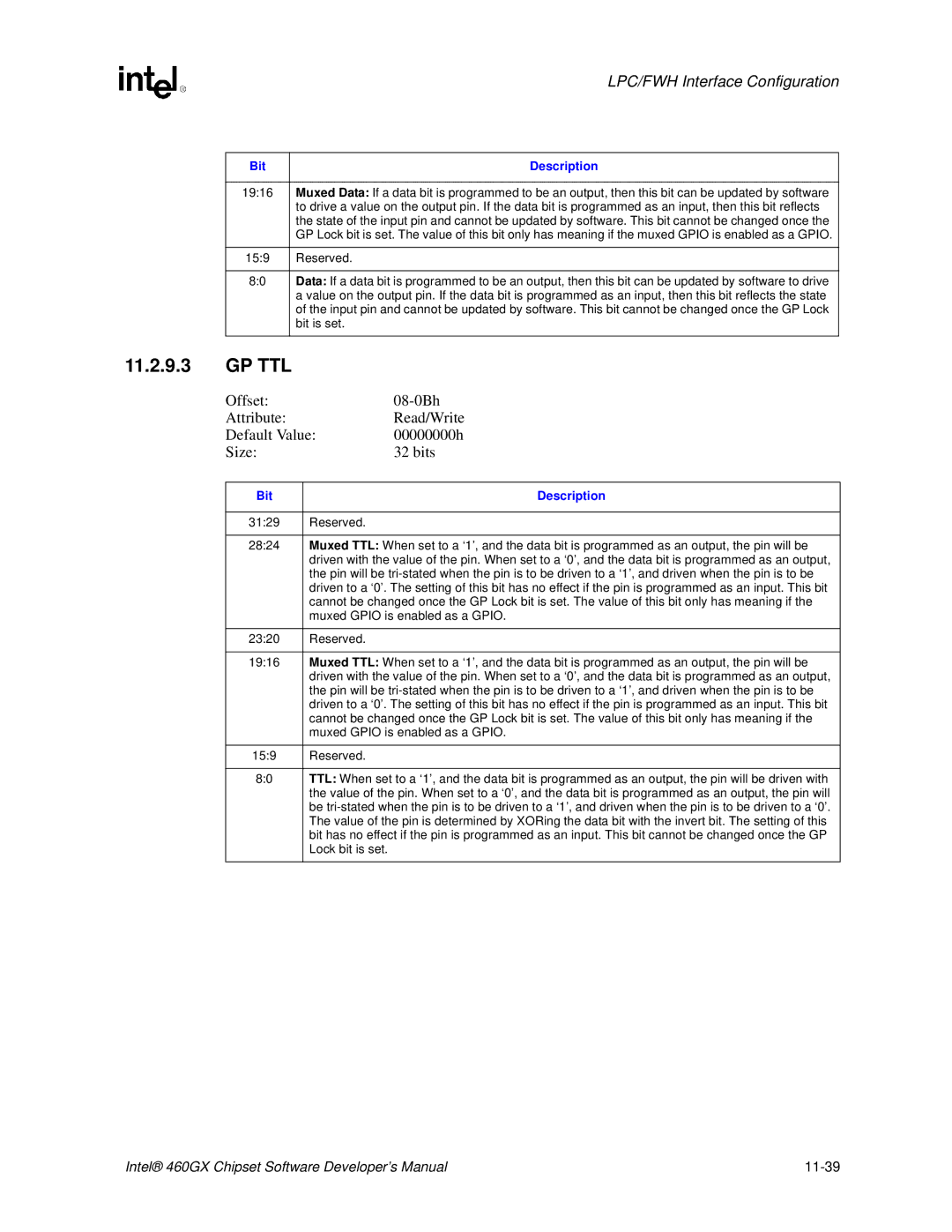
GP TTL
159 Reserved
Bit is set
GP Lock
GP Blink
GP Invert
GP Pulse
GP SMI
GP Core
GP Pull-up
11-42
PCI Configuration Registers Function
IDE Configuration
Configuration Mnemonic Register
IDE Controller Register Descriptions PCI Function
Wait Cycle Control. This bit is hardwired to
SERR# Enable. This bit is hardwired to
Parity Error Response. This bit is hardwired to
VGA Palette Snoop. This bit is hardwired to
By writing a 1 to this bit
SERR# Status. Read as
BMIBA-Bus Master Interface Base Address Register Function
MLT-Master Latency Timer Register Function
Bus Master interface registers and correspond to AD154
SID-Subsystem ID Function
SVID-Subsystem Vendor ID Function
IDETIM-IDE Timing Register Function
SIDETIM-Slave IDE Timing Register Function
Bit Description Reserved
DMACTL-Synchronous DMA Control Register Function
SDMATIM-Synchronous DMA Timing Register Function
Ultra DMA/33 Timing Mode Settings
BMICx-Bus Master IDE Command Register I/O
IDE Controller I/O Space Registers
Ultra DMA/33 Timing Modes
BMISx-Bus Master IDE Status Register I/O
Is equal to the IDE device transfer size
Interrupt/Activity Status Combinations
312
12-12
PCI Configuration Registers-Function
Universal Serial Bus USB Configuration
Usbren
Bit Description 1510 Reserved. Read
USB Host Controller Register Descriptions PCI Function
Reserved. Read as
Reserved. Read as 0’s
Resets STA to 0 by writing a 1 to this bit
Register in Function
This field
13-4
INTLN-Interrupt Line Register Function
USBBA-USB I/O Space Base Address Function
Miscellaneous Control Function
INTPN-Interrupt Pin Function
SBRNUM-Serial Bus Release Number Function
LEGSUP-Legacy Support Register Function
Needs to be serviced later
Default to 1 for compatibility with older USB software
Appropriate enable bits are set
Accesses that are part of the sequence
USBCMD-USB Command Register I/O
USBREN-USB Resume Enable
USB Host Controller I/O Space Registers
Swdbg Bit Run/Stop Bit Operation
Run/Stop, Debug Bit Interaction
Stop=0, the Frnum register can be reprogrammed
By Software or Hardware
USBSTS-USB Status Register I/O
USBINTR-USB Interrupt Enable Register I/O
Interrupt is generated to the system
Register =
FRNUM-Frame Number Register I/O
Address signals
FLBASEADD-Frame List Base Address Register I/O
SOFMOD-Start of Frame SOF Modify Register I/O
PORTSC-Port Status and Control Register I/O
Asserted, the corresponding port is disabled
X0 Disable
EOF2 time See of the USB Specification
Register define the hub states as follows
13-14
SM Bus Configuration Registers Function
SM Bus Controller Configuration
Class Code 0C-1Fh Reserved
Base Address Register
Shutdown special cycle
System Management Register Descriptions
14-2
STA to 0 by writing a 1 to this bit
14-4
SMBBA-SMBus Base Address Function
Interrupt pin PIRQB# is used
Host Configuration
SMBus I/O Space Registers
Smbslvc-SMBus Slave Command Function
Smbshdw1-SMBus Slave Shadow Port 1 Function
Smbshdw2-SMBus Slave Shadow Port 2 Function
Smbhststs-SMBus Host Status Register I/O
Transaction errors are caused by
Smbslvsts-SMBus Slave Status Register I/O
Position
Smbhstcnt-SMBus Host Control Register I/O
Command field of SMBus host transaction
Smbhstcmd-SMBus Host Command Register I/O
Smbhstadd-SMBus Host Address Register I/O
Smbhstdat0-SMBus Host Data 0 Register I/O
Smbblkdat-SMBus Block Data Register I/O
Smbhstdat1-SMBus Host Data 1 Register I/O
Smbslvcnt-SMBus Slave Control Register I/O
Smbslvdat-SMBus Slave Data Register I/O
14.3.9.1 Smbshdwcmd -SMBus Shadow Command Register I/O
14.3.9.2 10.3.11.smbslvevt-SMBus Slave Event Register I/O
Address 10h or one of the slave shadow port addresses
14-12
PCI Interface
PCI/LPC Bridge Description
Interrupt Controller
Programming the Interrupt Controller
Initialization Command Words ICWs
15-2
Automatic End of Interrupt Aeoi Mode
Operation Command Words OCWs
End of Interrupt Operation
End of Interrupt EOI
Special Fully Nested Mode
Fully Nested Mode
Modes of Operation
Automatic Rotation Equal Priority Devices
Poll Command
Cascade Mode
Specific Rotation Specific Priority
Special Mask Mode
Edge and Level Triggered Mode
Interrupt Masks
Masking on an Individual Interrupt Request Basis
Interrupt Steering
Reading the Interrupt Controller Status
Continuous Idle Mode
Quiet Active Mode
Serial Interrupts
Protocol
Serirq Frames
Stop Frame
Data Frame Number Usage # Clocks Past Start
3222
Programming the Interval Timer
Timer/Counters
15-10
Write Operations
Interval Timer Control Word Format
Read Operations
Counter Latch Command
Counter I/O Port Read
15-12
Real Time Clock
Read Back Command
RTC Standard RAM Bank
RTC Registers and RAM
Index Address Name
1 Invalid 0 Invalid
15.5.1.1 Register a
90625 ms 8125 ms
15.5.1.3 Register C
15.5.1.2 Register B
RSMRST#
RTC Interrupts
RTC Update Cycle
Lockable RAM Ranges
15.5.1.4 Register D
15-18
IFB Power States and Consumption
IFB Power Management
Overview
Acpi State Description
Power Plane Descriptions
IFB Power Planes
16.2.2 SMI# Generation
Causes of SMI#
Sleep States
SCI Generation
Causes of SCI#
SCI Event Comment
Entry/Exit for the S4 and S5 States
Acpi Bits Not Implemented by IFB
Acpi Bits Not Implemented in IFB
Offset Register Name/Function Comment
Action after Power Returns
Handling of Power Failures in IFB
S5 Wake Event Comment
16-6