Sink Core Interfaces

R

Sink Status and Flow Control Interface (Calendar Control and Status FIFO)

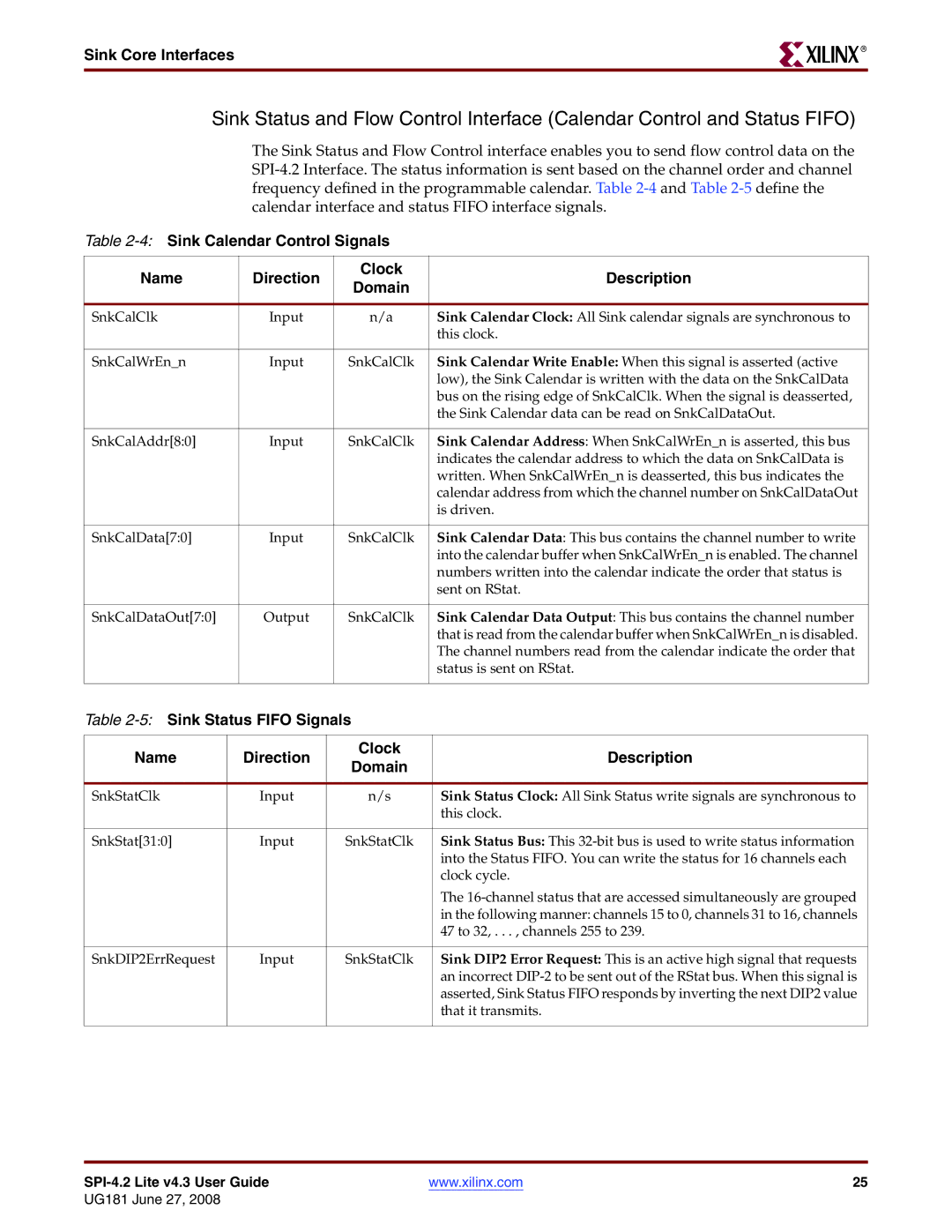
The Sink Status and Flow Control interface enables you to send flow control data on the SPI-4.2 Interface. The status information is sent based on the channel order and channel frequency defined in the programmable calendar. Table 2-4and Table 2-5define the calendar interface and status FIFO interface signals.

Table 2-4:Sink Calendar Control Signals

Name

Direction

Clock


Description

Domain


SnkCalClk

Input

n/a


Sink Calendar Clock: All Sink calendar signals are synchronous to


this clock.


SnkCalWrEn_n

Input

SnkCalClk


Sink Calendar Write Enable: When this signal is asserted (active


low), the Sink Calendar is written with the data on the SnkCalData


bus on the rising edge of SnkCalClk. When the signal is deasserted,


the Sink Calendar data can be read on SnkCalDataOut.


SnkCalAddr[8:0]

Input

SnkCalClk


Sink Calendar Address: When SnkCalWrEn_n is asserted, this bus


indicates the calendar address to which the data on SnkCalData is


written. When SnkCalWrEn_n is deasserted, this bus indicates the


calendar address from which the channel number on SnkCalDataOut


is driven.


SnkCalData[7:0]

Input

SnkCalClk


Sink Calendar Data: This bus contains the channel number to write


into the calendar buffer when SnkCalWrEn_n is enabled. The channel


numbers written into the calendar indicate the order that status is


sent on RStat.


SnkCalDataOut[7:0]

Output

SnkCalClk


Sink Calendar Data Output: This bus contains the channel number


that is read from the calendar buffer when SnkCalWrEn_n is disabled.


The channel numbers read from the calendar indicate the order that


status is sent on RStat.


Table 2-5:Sink Status FIFO Signals


Name


Direction


Clock


Description


Domain


SnkStatClk


Input


n/s


Sink Status Clock: All Sink Status write signals are synchronous to


this clock.


SnkStat[31:0]


Input


SnkStatClk


Sink Status Bus: This 32-bit bus is used to write status information


into the Status FIFO. You can write the status for 16 channels each


clock cycle.


The 16-channel status that are accessed simultaneously are grouped


in the following manner: channels 15 to 0, channels 31 to 16, channels


47 to 32, . . . , channels 255 to 239.


SnkDIP2ErrRequest


Input


SnkStatClk


Sink DIP2 Error Request: This is an active high signal that requests


an incorrect DIP-2 to be sent out of the RStat bus. When this signal is


asserted, Sink Status FIFO responds by inverting the next DIP2 value


that it transmits.


SPI-4.2 Lite v4.3 User Guide

www.xilinx.com

25

UG181 June 27, 2008

Page 25
Image 25
Xilinx UG181 manual Sink Core Interfaces

UG181 specifications

Xilinx UG181 refers to the User Guide for the Xilinx 7 Series FPGAs, which offers a comprehensive overview of the architecture, capabilities, and features of these powerful field-programmable gate arrays (FPGAs). Designed to cater to a wide range of applications, Xilinx 7 Series FPGAs are widely adopted in industries such as telecommunications, automotive, aerospace, and consumer electronics.

One of the main features of the Xilinx 7 Series FPGAs is their use of advanced 28nm technology, which enables them to achieve high performance while maintaining low power consumption. This fine process technology not only ensures better power efficiency but also allows for increased logic density. The 7 Series includes several families, such as Artix-7, Kintex-7, and Virtex-7, each tailored for specific application demands ranging from cost-sensitive solutions to high-performance data processing.

Xilinx 7 Series FPGAs also incorporate a rich set of programmable logic resources. This includes Look-Up Tables (LUTs), Flip-Flops, and Digital Signal Processing (DSP) slices that have been optimized for various arithmetic functions. With several thousands of logic cells available, designers can implement complex algorithms and systems directly in hardware for improved performance over traditional software solutions.

In addition to their logic capabilities, Xilinx 7 Series FPGAs feature an array of high-speed serial communication interfaces. These include support for technologies like PCI Express, Gigabit Ethernet, and Serial RapidIO, which facilitate efficient data transfer and integration into enterprise-level systems. The presence of high-speed transceivers also makes them ideal for applications that require fast data handling like video processing or high-frequency trading.

Furthermore, these FPGAs offer extensive memory options, including support for a wide range of external memory interfaces. This versatility allows for the integration of high-bandwidth memory solutions, which is essential for performance-intensive applications. With the introduction of the Memory Controller IP, users can easily connect various memory types, ensuring flexibility in system design.

Finally, Xilinx has made significant strides in development tools for 7 Series FPGAs, providing a robust ecosystem for design engineers. With design suites such as Vivado and SDK, users benefit from a comprehensive platform for deciding, simulating, and implementing designs efficiently. The combination of advanced hardware capabilities and powerful software tools solidifies the position of Xilinx 7 Series FPGAs as a preferred choice for custom digital hardware design across various industries.