Main
Document Number: MPC8260RM Rev. 2, 12/2005
How to Reach Us:
Page
Page
Page
Page
Page
Page
Page
Page
Page
Page
Page
Page
Page
Page
Page
Page
Page
Page
Page
Page
Page
Page
Page
Page
Page
Page
Page
Page
Page
Page
Page
Page
Page
Page
Page
Page
Page
Page
Page
Page
Page
Page
Page
Page
Page
Page
Page
Page
Page
Page
Page
Page
Page
Page
Page
Page
Page
Page
Page
Page
Page
Page
Page
Page
Page
Page
Page
Page
Page
Page
Page
Page
Page
Page
Page
Page
About This Book
Reference Manual Revision History
MPC8260 Family Reference Manual
Tablei. Changes to
, Rev. 1
Errata to MPC8260 Users Manual
Tableii. Device- and Silicon-Specific Notations
Before Using this ManualImport ant Note
Audience
Organization
Page
Page
Architecture Documentation
Page
Page
Page
Page
PowerPC Architecture Terminology Conventions
Tabl e v describes instruction field notation conventions used in this manual.
Tableiv. Terminology Conventions
Tablev. Instruction Fiel d Conventions
Page
Part I Overview
Tabl e I-1 contains acronyms and abbreviations that are used in this document.
TableI-1. Acronyms and Abbreviated Terms
TableI-1 . Acronyms and Abbreviated Terms (co ntinued)
Page
Chapter 1 Overview
1.1 Features
Page
Page
Page
Page
1.2 Architecture Overview
Freescale Semiconductor 1-7
Figure 1-1. PowerQUICC II Block Diagram
1.2.1 G2 Core
Notes:
1.2.2 System Interface Unit (SIU)
1.2.3 Communications Processor Module (CPM)
1.3 Software Compatibility Issues
1.3.1 Signals
Page
1.4 Differences between MPC860 and PowerQUICC II
1.5 Serial Protocol Table
1.6 PowerQUICC II Configurations
1.6.1 Pin Configurations
1.6.2 Serial Performance
1.7 Application Examples
1.7.1 Communication Systems
1.7.1.1 Remote Access Server
Page
1.7.1.2 Regional Office Router
1.7.1.3 LAN-to-WAN Bridge Router
Figure 1-5. LAN-to-WAN Bridge Router Configurat ion
1.7.1.4 Cellular Base Station
Figure 1-6. Cellular Base Station Configuration
1.7.1.5 Telecommunications Switch Controller
1.7.1.6 SONET Transmission Controller
1.7.2 Bus Configurations
1.7.2.1 Basic System
Figure 1-9. Basic System Configuration
Figure 1-10. High-Performance Communication
1.7.2.2 High-Performance Communication
Figure 1-10 shows a high-performance communication configuration.
1.7.2.3 High-Performance System Microprocessor
1.7.2.4 PCI
Figure 1-12. PCI Configuration
1.7.2.5 PCI with 155-Mbps ATM
Figure 1-13 shows the PCI with 155-Mbps ATM configuration (MPC8265 and MPC8266 only).
Figure 1-13. PCI with 155-Mbps ATM Configuration
1.7.2.6 PowerQUICC II as PCI Agent
Page
Chapter 2 G2 Core
2.1 Overview
Figure 2-1. PowerQUICC II Integrated Processor Core Block Diagram
2.2 G2 Processor Core Features
Page
2.2.1 Instruction Unit
2.2.2 Instruction Queue and Dispatch Unit
2.2.3 Branch Processing Uni t (BPU)
2.2.4 Independent Execution Units
2.2.4.1 Integer Unit (IU)
2.2.4.2 Floating-Point Unit (FPU)
2.2.4.3 Load/Store Unit (LSU)
2.2.4.4 System Register Unit (SRU)
2.2.5 Completion Unit
2.2.6 Memory Subsystem Support
2.2.6.1 Memory Management Units (MMUs)
2.2.6.2 Cache Units
2.3 Programming Model
2.3.1 Register Se t
2.3.1.1 PowerPC Register Set
Figure 2-2. PowerQUICC II Programming ModelRegisters
2.3.1.2 PowerQUICC II-Specific Registers
Page
Page
G2 Core Reference Manual
Figure 2-4. Hardware Implementation-Dependent Register 1 (HID1) Table2-2. HID1 Field Descriptions
Figure 2-5. Hardware Implementation-Dependent Register 2 (HID2) Table2-3. HID2 Field Descriptions
2.3.2 PowerPC Instruction Set and Addressing Modes
2.3.2.1 Calculating Effective Addresses
2.3.2.2 PowerPC Instruction Set
2.3.2.3 PowerQUICC II Implementation-Specific Instruction Set
2.4 Cache Implementation
2.4.1 PowerPC Cache Model
2.4.2 PowerQUICC II Implementation-Specific Cach e Implementation
2.4.2.1 Data Cache
Page
2.4.2.2 Instruction Cache
2.4.2.3 Cache Locking
2.5 Exception Model
2.5.1 PowerPC Exceptio n Model
2.5.2 PowerQUICC II Implementation-Specific Exceptio n Model
MPC603e Users Manual
Table2- 5. Exceptions and Conditio ns (continued)
2.5.3 Exception Priorities
2.6 Memory Management
2.6.1 PowerPC MMU Model
2.6.2 PowerQUICC II Implementation-Specific MMU Features
2.7 Instruction Timing
2.8 Differences between the PowerQUICC IIs G2 Core and the MPC603e Microprocessor
MPC603e Users Manual
MPC603e Users Manual
Table2-7. Major Differences between PowerQUICC IIs G2 Core and the
Chapter 3 Memory Map
Table3-1. Internal Memory Map
Page
Page
Page
Page
Page
Page
Page
Page
Page
Page
Page
Page
Page
Page
Page
Page
Page
Page
Page
Page
Page
Page
Page
Part II Configuration and Reset
Page
Chapter 4 System Interface Unit (SIU)
4.1 System Configuration and Protection
4.1.1 Bus Monitor
4.1.2 Timers Clock
4.1.3 Time Counter (TMCNT)
4.1.4 Periodic Interrupt Timer (PIT)
4.1.5 Software Watchdog Timer
4.2 Interrupt Controller
4.2.1 Interrupt Configuration
Figure 4-8. PowerQUICC II Interrupt Structure
4.2.1.1 Machine Check Interrupt
4.2.1.2 INT Interrupt
4.2.2 Interrupt Source Priorities
Table4-2. Interrupt Source Priority Levels
Table4-2. In terrupt Source Priority Levels (continued)
4.2.2.1 SCC, FCC, and MCC Relative Priority
4.2.2.2 PIT, TMCNT, PCI, and IRQ Relative Priority
4.2.2.3 Highest Priority Interrupt
4.2.3 Masking Interrupt Sources
Figure 4-9. Interrupt Request Masking
4.2.4 Interrupt Vector Generation and Calculation
Table4- 3. Encoding the Interrupt Vector
Table4- 3. Encoding the Interrupt Vector (continued)
4.2.4.1 Port C External Interrupts
4.3 Programming Model
4.3.1 Interrupt Controller Registers
4.3.1.1 SIU Interrupt Configuration Register (SICR)
The SICR register bits are described in Table 4 -4.
4.3.1.2 SIU Interrupt Priority Register (SIPRR)
Figure 4-11. SIU Interrupt Priority Register (SIPRR)
The SIPRR register bits are described in Table 4- 5.
Table4-4. SICR Field Descriptions
4.3.1.3 CPM Interrupt Priority Registers (SCPRR_H and SCPRR_L)
Figure 4-12. CPM High Interrupt Priority Register (SCPRR_H)
Tabl e 4-6 describes SCPRR_H fields.
Table4-5. SIPRR Field Descriptions
Tabl e 4-7 describes SCPRR_L fields.
Table4-6. SCPRR_H Field Descriptions
Figure 4-13. CPM Low Interrup t Priority Register (SCPRR_L)
4.3.1.4 SIU Interrupt Pending Registers (SIPNR_H and SIPNR_L)
Figure 4-14. SIPNR_H
Figure 4-15 shows SIPNR_L fields.
Table4-7. SCPRR_L Field Descriptions
4.3.1.5 SIU Interrupt Mask Registers (SIMR_H and SIMR_L)
Page
4.3.1.6 SIU Interrupt Vector Register (SIVEC)
Figure 4-19. Interrupt Table Handling Example
4.3.1.7 SIU External Interrupt Control Register (SIEXR)
Tabl e 4-8 describes SIEXR fields.
4.3.2 System Configuration and Protection Registers
The system configuration and protection registers are described in the following sections.
4.3.2.1 Bus Configuration Register (BCR)
Figure 4-20. SIU External Interrupt Control Register (SIEXR) Table4- 8. SIEXR Field Descriptions
Figure 4-9 describes BCR fields.
Figure 4-21. Bus Configuration Register (BCR) Table4-9. BCR Field Descriptions
Table4- 9. BCR Field Descriptions ( continued)
4.3.2.2 60x Bus Arbiter Configuration Register (PPC_ACR)
Figure4-22. PPC_ACR
Table4-10 describes PPC_ACR fields.
Table4- 9. BCR Field Descriptions ( continued)
4.3.2.3 60x Bus Arbitration-Level Registers (PPC_ALRH/PPC_ALRL)
Figure 4-23. PPC_ALRH
Table4-10. PPC_ACR Field Descriptions
4.3.2.4 Local Bus Arbiter Configuration Register (LCL_ACR)
Table4-11 describes LCL_ACR register bits.
Figure 4-24. PPC_ALRL
Figure 4-25. LCL_ACR Table4-11. LCL_ACR Field Descriptions
4.3.2.5 Local Bus Arbitration Level Registers (LCL_ALRH and LCL_ACRL)
Figure4-26. LCL_ALRH
Table4-11. LCL_ACR Field Descriptions (continued)
4.3.2.6 SIU Module Configuration Register (SIUMCR)
Table4-12 describes SIUMCR fields.
Figure 4-27. LCL_ALRL
Figure4-28. SIU Model Configuration Register (SIUMCR) Table4-12. SIUMCR Register Field Descriptions
Page
Table4-12. SIUMCR Register Field Descriptions (continued)
4.3.2.7 Internal Memory Map Register (IMMR)
4.3.2.8 System Protection Control Register (SYPCR)
Figure 4-30. System Protection Control Register (SYPCCR)
Table4-13. IMMR Field Descriptions
Table4-14 describes SYPCR fields.
4.3.2.9 Software Service Register (SWSR)
The 60x bus transfer error status and control register 1 (TESCR1) is shown in Figure 4-31.
4.3.2.10 60x Bus Transfer Error Status and Control Register 1 (TESCR1)
Table4-14. SYPCR Field Descriptions
Table4-15 describes TESCR1 fields.
4.3.2.11 60x Bus Transfer Error Status and Control Register 2 (TESCR2)
The 60x bus transfer error status and control register 2 (TESCR2) is shown in Figure 4-32.
Table4-15. TESCR1 Field Descriptions (continued)
The TESCR2 register is described in Table 4-16.
4.3.2.12 Local Bus Transfer Error Status and Control Register 1 (L_TESCR1)
The local bus transfer error status and control register 1 (L_TESCR1) is shown in Figure4-33.
The L_TESCR1 register bits are described in Table4-17.
4.3.2.13 Local Bus Transfer Error Status and Control Register 2 (L_TESCR2)
The local bus transfer error status and control register 2 (L_TESCR2) is shown in Figure4-34.
Table4-18 describes L_TESCR2 fields.
Table4-17. L_TESCR1 Field Descriptions (continued)
4.3.2.14 Time Counter Status and Control Register (TMCNTSC)
Table4-19 describes TMCNTSC fields.
4.3.2.15 Time Counter Register (TMCNT)
4.3.2.16 Time Counter Alarm Register (TMCNTAL)
Table4-20 describes TMCNTAL fields.
Figure 4-36. Time Counter Register (TCMCNT)
Figure 4-37. Time Counter Alarm Register (TMCNTAL) Table4-20. TMCNTAL Field Descriptions
4.3.3 Periodic Interrupt Registers
4.3.3.1 Periodic Interrupt Status and Control Register (PISCR)
4.3.3.2 Periodic Interrupt Timer Count Register (PITC)
Table4-22 describes PITC fields.
4.3.3.3 Periodic Interrupt Timer Register (PITR)
Figure4-40. Periodic Interrupt Timer Register (PITR)
Figure 4-39. Periodic interrupt Time r Count Register (PITC) Table4-22. PITC Field Descriptions
4.3.4 PCI Control Registers
4.3.4.1 PCI Base Register (PCIBRx)
Table4-24 describes PCIBRx fields.
4.3.4.2 PCI Mask Register (PCIMSKx)
Figure 4-42 shows the PCI mask register.
4.4 SIU Pin Multiplexing
Table4-24. PCIBRx Field Descriptions
Table4-25. PCIM SKx Field Descriptions
4-50 Freescale Semiconductor
Table4-26. SIU Pins Multiplexing Control
Pin Name Pin Configuration Control
Chapter 5 Reset
5.1 Reset Causes
5.1.1 Reset Actions
5.1.2 Power-On Reset Flow
5.1.3 HRESET Flow
5.1.4 SRESET Flow
5.2 Reset Status Register (RSR)
Tabl e 5-3 describes RSR fields.
Figure 5-2. Reset Status Register (RSR) Table5-3. RSR Field Descriptions
5.3 Reset Mode Register (RMR)
5.4 Reset Configuration
Page
5.4.1 Hard Reset Configuration Word
The contents of the hard reset configuration word are shown in Figure5-4.
n_nnnn
nnnnn
Tabl e 5-7 describes hard reset configuration word fields.
Table5- 7. Hard Reset Configuration Word Field Descriptions (cont inued)
5.4.2 Hard Reset Configuration Examples
5.4.2.1 Single PowerQUICC II with Default Configuration
5.4.2.2 Single PowerQUICC II Configured from Boot EPROM
5.4.2.3 Multiple PowerQUICC IIs Configured from Boot EPROM
Figure5-7. Configuring Multiple Chips
5.4.2.4 Multiple PowerQUICC IIs in a System with No EPROM
Page
Part III The Hardware Interface
Page
Page
TableIII-1. Acronyms and Abbreviated Terms (continued)
Chapter 6 External Signals
6.1 Functional Pinout
6.2 Signal Descriptions
Table6-1 . External Signals
Page
Page
Page
Page
Page
Page
Page
Page
Page
Page
Page
Page
Page
Chapter 7 60x Signals
7.1 Signal Configuration
Figure shows the grouping of the PowerQUICC IIs 60x bus signal configuration.
Figure 7-1. Signal Groupings
7.2 Signal Descriptions
7.2.1 Address Bus Arbitration Sig nals
7.2.1.1 Bus Request (BR)Output
7.2.1.2 Bus Grant (BG)
7.2.1.3 Address Bus Busy (ABB)
7.2.2 Address Transfer Start Signal
7.2.2.1 Transfer Start (TS)
7.2.2.2 Transfer Start (TS)Input
7.2.3 Address Transfer Signals
7.2.3.1 Address Bus (A[031])
7.2.4 Address Transfer Attribute Signals
7.2.4.1 Transfer Type (TT[04])
7.2.4.2 Transfer Size (TSIZ[03])
7.2.4.3 Transfer Burst (TBST)
7.2.4.4 Global (GBL)
7.2.4.5 Caching-Inhibited (CI)Output
7.2.4.6 Write-Through (WT)Output
7.2.5 Address Transfer Termination Sig nals
7.2.5.1 Address Acknowledge (AACK)
7.2.5.2 Address Retry (ARTRY)
7.2.6 Data Bus Arbitration Signals
7.2.6.1 Data Bus Grant (DBG)
7.2.6.2 Data Bus Busy (DBB)
7.2.7 Data Transfer Signals
7.2.7.1 Data Bus (D[063])
7.2.7.2 Data Bus Parity (DP[07])
7.2.8 Data Transfer Termination Sig nals
7.2.8.1 Transfer Acknowledge (TA)
Page
7.2.8.2 Transfer Error Acknowledge (TEA)
7.2.8.3 Partial Data Valid Indication (PSDVAL)
Page
Page
Chapter 8 The 60x Bus
8.1 Terminology
8.2 Bus Configuration
8.2.1 Single-PowerQUICC II Bus Mode
8.2.2 60x-Compatible Bus Mode
Figure 8-2. 60x-Compatible Bus Mode
8.3 60x Bus Protocol Overview
8.3.1 Arbitration Phase
8.3.2 Address Pipelining and Split-Bus Transactions
8.4 Address Tenure Operations
8.4.1 Address Arbitration
8.4.2 Address Pipelining
8.4.3 Address Transfer Attribute Signals
8.4.3.1 Transfer Type Signal (TT[04]) Encoding
Table 8-2. Tran sfer Type Enco din g
Regarding Tabl e 8-2:
Table8-2. Transfer Type Encoding (continued)
8.4.3.2 Transfer Code Signals TC[02]
8.4.3.3 TBST and TSIZ[03] Signals and Size of Transfer
8.4.3.4 Burst Ordering During Data Transfers
Each data beat is terminated with an assertion of TA.
8.4.3.5 Effect of Alignment on Data Transfers
Table8-5. Burst Ordering
Table 8-6. Aligned Da ta Transfers
Page
8.4.3.6 Effect of Port Size on Data Transfers
Figure 8-6. Interface to Different Port Size Devices
8.4.3.7 60x-Compatible Bus ModeSize Calculation
Table8-8. Data Bus: Rea d Cycle Requirements and Write Cycle Content
8.4.3.8 Extended Transfer Mode
Table8-9. Address and Size State Calculations
Table8-10. Data Bus Contents for Extended Write Cycles
Table8-11. Data Bus Requirements for Extended Read Cycles
Table8-12. Address and Size State for Extended Transfers
8.4.4 Address Transfer Termination
8.4.4.1 Address Retried with ARTRY
Page
8.4.4.2 Address Tenure Timing Configuration
8.4.5 Pipeline Control
8.5 Data Tenure Operations
8.5.1 Data Bus Arbitra tion
8.5.2 Data Streaming Mode
8.5.3 Data Bus Transfers and Normal Termination
8.5.4 Effect of ARTRY Assertion on Data Transfer and Arbi tration
8.5.5 Port Size Data Bus Transfers and PSDVAL Termination
Figure 8-9. 28-Bit Extended Transfer to 32-Bit Port Size
8.5.6 Data Bus Termination by Assertion o f TEA
8.6 Memory CoherencyMEI Protocol
8.7 Processor State Signals
8.7.1 Support for the lwarx/stwcx. Inst ruction Pair
8.7.2 TLBISYNC Input
8.8 Little-Endian Mode
Chapter 9 PCI Bridge
Figure9-1. PCI Bridge in the PowerQUICC II
Figure 9-2. PCI Bridge Structure
9.1 Signals
9.2 Clocking
9.3 PCI Bridge Initialization
9.4 SDMA Interface
9.5 Interrupts from PCI Bridge
9.6 60x Bus Arbitration Priority
9.7 60x Bus Maste rs
9.8 CompactPCI Hot Swap Specification Support
9.9 PCI Interface
9.9.1 PCI Interface Operation
9.9.1.1 Bus Commands
9.9.1.2 PCI Protocol Fundamentals
Table9- 2. PCI Command Definitions
Page
9.9.1.3 Bus Transactions
Page
Page
Page
9.9.1.4 Other Bus Operations
Page
Page
Page
9.9.1.5 Error Functions
Page
9.9.2 PCI Bus Arbitration
9.9.2.1 Bus Parking
9.9.2.2 Arbitration Algorithm
9.9.2.3 Master Latency Timer
9.10 Address Map
Page
Page
9.10.1 Address Map Programming
9.10.2 Address Translation
9.10.2.1 PCI Inbound Translation
9.10.2.2 PCI Outbound Translation
9.10.3 SIU Registers
9.11 Configuration Registers
9.11.1 Memory-Mapped Configuration Registers
Page
Table9-3. Internal Memory Map (continued)
9.11.1.1 Message Unit (I2O) Registers
9.11.1.2 DMA Controller Registers
9.11.1.3 PCI Outbound Translation Address Registers (POTAR
)
9.11.1.4 PCI Outbound Base Address Registers (POBAR
)
9.11.1.5 PCI Outbound Comparison Mask Registers (POCMR
)
Figure 9-19. PCI Outbound Comparison Mask Registers (POCMR
9.11.1.6 Discard Timer Control Register (PTCR)
Field Descriptions
Figure 9-20. Discard Timer Control register (PTCR)
Table9-7. describes PTCR fields.
9.11.1.7 General Purpose Control Register (GPCR)
Table9-7. PTCR Field Descriptions
Figure9-21. General Purpose Control Register (GPCR)
Table9-8. describes GPCR fields.
Table9- 8. GPCR Field Descriptions
9.11.1.8 PCI General Control Register (PCI_GCR)
Figure 9-22. PCI General Control Register (PCI_GCR)
Table9-9. describes PCI_GCR fields.
9.11.1.9 Error Status Register (ESR)
Table9- 9. PCI_GCR Field Descriptions
Table9-10. describes ESR fields.
Table9- 10. ESR Field Descriptions
9.11.1.10 Error Mask Register (EMR)
Table9-11. describes EMR fields.
Figure 9-24. Error Mask Register (EMR)
Table9-11. EMR Field Descriptions
Table9-10. ESR F ield Descriptions (continued)
9.11.1.11 Error Control Register (ECR)
Table9-12 describes ECR fields.
Figure 9-25. Error Control Registe r (ECR)
Table9-11. EMR Field Descriptions (continued)
9.11.1.12 PCI Error Address Capture Register (PCI_EACR)
Table9-13. describes PCI_EACR f ields.
Figure9-26. PCI Error Address Capture Register (PCI_EACR)
Table9-12. ECR Field De scriptions
9.11.1.13 PCI Error Data Capture Register (PCI_EDCR)
9.11.1.14 PCI Error Control Capture Register (PCI_ECCR)
Figure 9-28. PCI Error Control Capture Register (PCI_ECCR)
Table9-15 describes PCI_ECCR fields.
Table9-15. PCI_ECCR Field Descriptions
Table9-10
9.11.1.15 PCI Inbound Translation Address Registers (PITAR
)
Table 9-1 6. PI TAR
9.11.1.16 PCI Inbound Base Address Registers (PIBAR
Figure 9-29. PCI Inbound Translation Address Registers (PITAR
9.11.1.17 PCI Inbound Comparison Mask Registers (PICMR
)
Figure 9-31. PCI Inbound Comparison Mas k Registers (PICMR
Table9-18. describes PICMRx.
Table9-18. PICMR
x)
x
9.11.2 PCI Bridge Configuration Registers
Figure9-32. PCI Bridge PCI Configuration Registers
9.11.2.1 Vendor ID Register
Figure 9-33 and Table9-20 describe the vendor ID register.
Table9-19. PCI Bridge PCI Configuration Registers (continued)
Figure 9-33. Vendor ID Register
9.11.2.2 Device ID Register
Figure 9-35. PCI Bus Command Register
Figure 9-34 and Table9-21 describes the device ID register.
Figure 9-34. Device ID Register
9.11.2.3 PCI Bus Command Register
9.11.2.4 PCI Bus Status Register
Table9-22. PCI B us Command Register Description
Figure 9-36. PCI Bus Status Register
Table9-23. describes the PCI bus status register fields.
9.11.2.5 Revision ID Register
Figure 9-37 and Table9-24 describe the revision ID register.
Table9-23. PCI Bus Status Register Description
Figure 9-37. Revision ID Register
9.11.2.6 PCI Bus Programming Interface Register
Figure 9-38 and Table9-25 describe the PCI bus pr ogramming interface register.
Figure 9-39 and Table9-26 describe the subclass code register.
Figure 9-38. PCI Bus Programming Interface Register
9.11.2.7 Subclass Code Register
9.11.2.8 PCI Bus Base Class Code Register
9.11.2.9 PCI Bus Cache Line Size Register
Figure 9-41. PCI Bus Cache Line Size Register
9.11.2.10 PCI Bus Latency Timer Register
Figure 9-42 and Table9-29 describe the PCI bus latency timer register.
Figure 9-43 and Table9-30 describe the header type register.
Figure 9-42. PCI Bus Latency Timer Register
9.11.2.11 Header Type Register
9.11.2.12 BIST Control Register
9.11.2.13 PCI Bus Internal Memory-Mapped Registers Base Address Register (PIMMRBAR)
9.11.2.14 General Purpose Local Access Base Address Registers (GPLABAR
)
Figure 9-46. General Purpose Local Access Base Address Reg isters (GPLABAR
Table9-33 describes GPLABARx fields.
Table9-33. GPLABAR
9.11.2.15 Subsystem Vendor ID Register
Figure 9-47 and Table9-34 describe the subsystem vendor ID register.
9.11.2.16 Subsystem Device ID Register
Figure 9-48 and Table9-35 describe the subsystem ID register.
Figure 9-50 and Table9-37 describes the PCI bus interrupt line register.
Figure 9-48. Subsystem Device ID Register
9.11.2.17 PCI Bus Capabilities Pointer Register
9.11.2.19 PCI Bus Interrupt Pin Register
Figure9-52. PCI Bus MIN GNT
Figure 9-51 and Table9-38 describe the PCI bus interrupt pin register.
Figure 9-51. PCI Bus Interrupt Pin Register
9.11.2.20 PCI Bus MIN GNT
9.11.2.21 PCI Bus MAX LAT
Figure 9-53 and Table9-40 describe the PCI bus MAX LAT register.
Table9-41. describes PCI bus function register fields.
Figure 9-53. PCI Bus MAX LAT
9.11.2.22 PCI Bus Function Register
9.11.2.23 PCI Bus Arbiter Configuration Register
Figure 9-55. PCI Bus Arbiter Configuration Register
Table9-41. PCI Bu s Function Register Field Descriptions
Table9-42. describes the PCI bus arbiter configuration register fields.
9.11.2.24 PCI Hot Swap Register Block
Table9-43 describes the Hot Swap register block fields.
Figure 9-56. Hot Swap Register Block
Table9-42. P CI Bus Arbiter Configuration Register Field Description
9.11.2.25 PCI Hot Swap Control Status Register
Figure 9-57 and Table9-44 describe the Hot Swap control status register.
Figure 9-57. Hot Swap Control Status Register
Table9-43. Hot Swap Register Block Field Descriptions
Table9-44. Hot Swap Control Status Register Field Descriptions
9.11.2.26 PCI Configuration Register Access from the Core
Example: configuration sequence, 2-byte data write to register at address offset 0x1A for PCI bus.
Page
9.11.2.28 Initializing the PCI Configuration Registers
9.12 Message Unit (I2O)
9.12.1 Messag e Registers
9.12.1.1 Inbound Message Registers (IMR
)
9.12.1.2 Outbound Message Registers (OMR
)
9.12.2 Door Bell Registers
9.12.2.1 Outbound Doorbell Register (ODR)
Figure 9-62. Outbound Doorbel l Register (ODR)
9.12.2.2 Inbound Doorbell Register (IDR)
Figure 9-63. Inbound Doorbell Regist er (IDR)
Table9-48. ODR Field Descriptions
9.12.3 I2O Unit
Figure 9-64. I2O Message Queue
9.12.3.1 PCI Configuration Identification
9.12.3.2 Inbound FIFOs
Page
Page
Figure 9-67. Inbound Post_FIFO Head Pointer Register (IPHPR)
Figure 9-68. Inbound Post_FIFO Tail Pointer Register (IPTPR)
Table9-52. IPHPR F ield Descriptions
9.12.3.3 Outbound FIFOs
Page
Page
Figure 9-72. Outbound Post_FIFO Tail Pointer Register (OPTPR)
9.12.3.4 I2O Registers
Figure 9-73. Inbound FIFO Queue Port Regist er (IFQPR)
Table9-57. OPTPR Field Descriptions
Page
Figure 9-75. Outbound Message Interrupt Status Register (OMISR)
Table9-60 describes OMISR fields.
Table9-60. OMISR Field Descriptions
Figure 9-76. Outbound Message Interrupt Mask Register (OMIMR)
Table9-61 describes OMIMR f ields.
Table9-61. O MIMR Field Descriptions
Figure 9-77. Inbound Message Interrupt Status Register (IMIS R)
Table9-62 describes IMISR fields.
Table9- 62. IMISR Field Descriptions
Figure 9-78. Inbound Message Interrupt Mask Register (I MIMR)
Table9-63 describes IMIMR fields.
Table9-63. IMIMR Field Descriptions
Figure 9-79. Messaging Unit Control Register (MUCR)
Table9-64 describes MUCR fields.
Table9-64. MUCR Field Descriptions
Table9-63. IMIMR Field Descriptions (continued)
Figure 9-80. Queue Base Address Register (QBAR)
Table9-65 describes QB AR fields.
Table9-65. Q BAR Field Descriptions
Table9-64. MUCR Field Descriptions
9.13 DMA Controller
9.13.1 DMA Operat ion
9.13.1.1 DMA Direct Mode
9.13.1.2 DMA Chaining Mode
9.13.1.3 DMA Coherency
9.13.1.4 Halt and Error Conditions
9.13.1.5 DMA Transfer Types
9.13.1.6 DMA Registers
Table 9-66 . DM AMR
Field Descriptions
Channels.
9.13.1.6.2 DMA Status Register [03] (DMASR
Table 9-66 . DM AMR
Table9-67 describes DMASRx fields.
Figure 9-83. DMA Status Register [03] (DMASR
Field Descriptions (continued)
9.13.1.6.3 DMA Current Descriptor Address Register [03] (DMACDAR
Table9-67. DMASR
Table9-68 describes DMACDARx fields.
Figure 9-84. DMA Current Descriptor Address Register [03] (DMACDAR
Field Descriptions
Page
Page
9.13.1.6.7 DMA Next Descriptor Address Register [03] (DMANDAR
Table9-71. DMABCR
Table9-72. DMANDAR
Table9-72 describes DMANDARx fields.
Figure 9-88. DMA Next Descriptor Address Register [03] (DMANDAR
9.13.2 DMA Segment Descriptors
Figure 9-89. DMA Chain of Segment Descriptors
9.13.2.1 Descriptor in Big Endian Mode
9.13.2.2 Descriptor in Little Endian Mode
9.14 Error Handling
9.14.1 Interrupt and Error Signals
9.14.1.1 PCI Bus Error Signals
9.14.1.2 Illegal Register Access Error
9.14.1.3 PCI Interface
Page
9.14.1.4 Embedded Utilities
Chapter 10 Clocks and Power Control
10.1 Clock Unit
10.2 Clock Configuration
10.3 External Clock Inputs
10.4 Main PLL
10.4.1 PLL Block Diagra m
10.4.2 Skew Elimination
10.4.3 PCI Bridge Clocking
10.4.3.1 PCI Bridge as an Agent Operating from the PCI System Clock
Figure 10-2. PCI Bridge as an Agent, Operating from the PCI System Clock
10.4.3.2 PCI Bridge as a Host and Generating the PCI System Clock
Figure 10-3. PCI Bridge as a Host, Generating the PCI S ystem Clock
10.5 Clock Dividers
10.6 PowerQUICC II Internal Clock Signals
10.6.1 General System Clocks
10.7 PLL Pins
Table10-1 shows dedicated PLL pins .
Table10-1. Dedicated PLL Pins
Figure 10-4 shows the filtering circuit for VCCSYN and VCCSYN1, described in Table10- 1.
Figure 10-4. PLL Filtering Circuit
Table10 -1. Dedicated PLL Pins (continued)
.29m (HiP3) Silicon: Rev. A.1 and B.x
.29m (HiP3) Silicon: Rev. C.2 and Future Revisions
10.8 System Clock Control Register (SCCR)
Table10-2 describes SCCR fields.
Figure 10-5. System Clock Control Register (SCCR) Table10-2. SCCR Field Descriptions
10.9 System Clock Mode Register (SCMR)
Figure 10-6. System Clock Mode Register (SCMR)
Table10-2. SCCR Field D escriptions (continued)
The relationships among these parameters are described in the formulas in Figure10-7.
Figure 10-7. Relationships of SCMR Paramet ers
SCMR[CORECNF] bit values are shown in Table10-4.
Table10-3. SCMR Field Descriptions
10.10 Basic Power Structure
Table10-4. 60x Bus-to-Core Frequency
Page
Chapter 11 Memory Controller
Figure 11-1. Dual-Bus Architecture
11.1 Features
11.2 Basic Architecture
Page
Page
11.2.1 Address and Address Space Checking
11.2.2 Page Hit Checking
11.2.3 Error Checking and Correction (ECC )
11.2.4 Parity Generation and Checking
11.2.5 Transfer Error Acknowledge (TEA) Generation
11.2.6 Machine Check Interrupt (MCP) Generati on
11.2.7 Data Buffer Controls (BCTL
and LWR)
11.2.8 Atomic Bus Operation
11.2.9 Data Pipelining
11.2.10 E xternal Memory Controller Support
11.2.11 E xternal Address Latch Enable Signal (ALE)
11.2.12 E CC/Parity Byte Select (PBSE)
11.2.13 Partial Data Valid Indication (PSDVAL)
11.2.14 BADDR[27:31] Signal Connections
Table11-3 lists registers used to control the 60x bus memory controller.
11.3 Register Descriptions
Table11-2. BADDR Connections
Table11-3. 60x B us Memory Controller Registers
11.3.1 Base Registers (BR
Figure 11-6. Base Registers (BR
Table11-4 describes BRx fields.
Table11-4. BR
11.3.2 Option Registers (OR
Table11-5. OR
Field Descriptions (SDRAM Mode)
Figure 11-8 shows ORx as it is formatted for GPCM mode.
Table11-5. OR
Figure 11-8. OR
Table11-6 describes ORx fields in GPCM mode.
GPCM Mode Table11-6. OR
Table11-6. OR
GPCM Mode Field Descriptions (continued)
Figure 11-9. OR
Table11-7 describes the ORx fields in UPM mode.
UPM Mode Table11-7. Option Reg ister (OR
)UPM Mode
11.3.3 60x SDRAM Mode Register (PSDMR)
Figure 11-10. 60x/Local SDRAM Mode Register (PSDMR/LSDMR)
Table11-8 describes PSDMR fields. LSMDR fields a re described in Table 11-9..
Table11-7. Option Reg ister (OR
)UPM Mode
Table11-8. PSDMR Field Descriptions
Table11-8. PSDMR Field Descriptions (continued)
11.3.4 Local Bus SDRAM Mode Register (LSDMR)
Table11-9. LSDMR Field Descriptions
Table11-8. PSDMR Field Descriptions (continued)
Page
Page
11.3.5 Machine A/B/C Mode Registers (M
MR)
Mode Registers (M
Figure 11-11. Machine
Table11-10 describes MxMR bits.
Table11-10. Machine x Mode Registers (M
11.3.6 Memory Data Register (MDR)
Table11-10. Machine x Mode Registers (M
MR) (continued)
Table11-11 describes MDR fields.
11.3.7 Memory Address Register (MAR)
Figure 11-13. Memory Address Register (MAR)
Table11-12 describes MAR fields.
The memory address register (MAR) is shown in Figure 11-13.
Figure 11-12. Memory Data Register (MDR) Table11-11. MDR Field Descriptions
11.3.8 60x Bus-Assigned UPM Refres h Timer (PURT)
The 60x bus assigned UPM refresh timer register (PURT) is shown in Figure11-14.
Table11-14 describes LURT fields.
Table11-13 describes PURT fields.
11.3.9 Local Bus-Assigned UPM Re fresh Timer (LURT)
11.3.10 60x Bus-Assigned SDRAM Refresh Timer (PSRT)
The 60x bus assigned SDRAM refresh timer register (PSRT) is shown in Figure 11-16.
The local bus-assigned SDRAM refresh timer register (LSRT) is shown in Figure11-17.
Table11-15 describes PSRT fields.
11.3.11 Local Bus-Assigned SDRAM Refresh Timer (LSRT)
11.3.12 Memory Refresh Timer Pres caler Register (MPTPR)
bus
Table11-17 describes MPTPR fields.
Figure 11-18 shows the memory refresh timer prescaler register (MPTPR).
Figure 11-17. Local Bus-Assigned SDRAM Refresh Timer (LSRT) Table11-16. LSRT Field Descr iptions
11.4 SDRAM Machine
Figure 11-19. 128-Mbyte SDRAM (Eight-Bank Configuration, Banks 1 and 8 Shown)
11.4.1 Supported SDRAM Configurations
11.4.2 SDRAM Power-On Initialization
11.4.3 JEDEC-Standard SDRAM Interface Commands
11.4.4 Page-Mode Support and Pipeline Accesses
Table11-19. SDRAM Interface Commands
11.4.5 Bank Interleaving
11.4.5.1 Using BNKSEL Signals in Single-PowerQUICCII Bus Mode
11.4.5.2 SDRAM Address Multiplexing (SDAM and BSMA)
11.4.6 SDRAM Device-Specific Parameters
11.4.6.1 Precharge-to-Activate Interval
11.4.6.2 Activate to Read/Write Interval
11-40 Freescale Semiconductor
Figure 11-21. ACTTORW = 2 (2 Clock Cycles)
11.4.6.3 Column Address to First Data OutCAS Latency
Figure 11-22. CL = 2 (2 Clock Cycles)
Freescale Semiconductor 11-41
11.4.6.4 Last Data Out to Precharge
Figure 11-24. WRC = 2 (2 Clock Cycles)
Figure 11-23. LDOTOPRE = 2 (-2 Clock Cycles)
11.4.6.5 Last Data In to PrechargeWrite Recovery
11.4.6.6 Refresh Recovery Interval (RFRC)
11.4.6.7 External Address Multiplexing Signal
11.4.6.8 External Address and Command Buffers (BUFCMD)
Freescale Semiconductor 11-43
Figure11-27. BUFCMD = 1
11.4.7 SDRAM Interface Timing
Figure 11-28 through Figure11-36 show SDRAM timing for various types of acce sses.
11-44 Freescale Semiconductor
Figure 11-29. SDRAM Single-Beat Read, Page Hit, CL = 3
Figure 11-30. SDRAM Two-Beat Burst Read, Page Closed, CL = 3
Figure 11-31. SDRAM Four-Beat Burst Read, Page Miss, CL = 3
Freescale Semiconductor 11-45
Figure 11-32. SDRAM Single-Beat Write, Page Hit
Figure 11-33. SDRAM Three-Beat Burst Write, Page Closed
Figure 11-34. SDRAM Read-after-Read Pipeline, Page Hit, CL = 3
11.4.8 SDRAM Read/Write Transactions
11.4.9 SDRAM MODE-SET Command Timing
11.4.10 SDRAM Refresh
11.4.11 SDRAM Refresh Timing
11.4.12 SDRAM Configuration Examples
11.4.12.1 SDRAM Configuration Example (Page-Based Interleaving)
11.4.13 SDRAM Configuration Example (Bank-Based Interleaving)
11.5 General-Purpose Chip-Select Machine (GPCM)
Table11-27. SDRAM Device Address Port during ACTIVATE Command
Table11-28. SDRAM Device Address Port during READ/WRITE Command
Table11-29. Register Settings (Bank-Based Interleaving)
Page
11.5.1 Timing Configuration
11.5.1.1 Chip-Select Assertion Timing
11.5.1.2 Chip-Select and Write Enable Deassertion Timing
Page
Figure 11-45. GPCM Memory Device Basic Timing (ACS 00, CSNT = 1, TRLX = 0)
11.5.1.3 Relaxed Timing
Figure 11-46. GPCM Relaxed Timing Read (ACS = 1x, SCY = 1, CSNT = 0, TRLX= 1)
Figure 11-47. GPCM Relaxed-Timing Write (ACS = 1x, SCY = 0, CSNT = 0,TRLX = 1)
Figure 11-48. GPCM Relaxed-Timing Write (ACS = 10, SCY = 0, CSNT = 1, TRLX = 1)
11.5.1.4 Output Enable (OE) Timing
11.5.1.5 Programmable Wait State Configuration
11.5.1.6 Extended Hold Time on Read Accesses
[2930] = 00, Fastest Timing)
Figure 11-50. GPCM Read Followed by Read (OR
See Figure 11-50 through Figure 11-53 for timing examples.
Table11-32. TRLX and EHTR Combinations
Figure 11-51. GPCM Read Followed by Read (OR
[2930] = 01)
Figure 11-52. GPCM Read Followed by Write (OR
11.5.2 External Access Termination
11.5.3 Boot Chip-Select Operation
11.5.4 Differences between MPC8xxs GPCM and MPC82xxs GPCM
11.6 User-Programmable Machines (UPMs)
11.6.1 Requests
Page
11.6.1.1 Memory Access Requests
11.6.1.2 UPM Refresh Timer Requests
11.6.1.3 Software RequestsRUN Command
11.6.1.4 Exception Requests
11.6.2 Programming the UPMs
11.6.3 Clock Timing
Page
11.6.4 The RAM Array
Figure 11-61. RAM Array and Signal Generation
11.6.4.1 RAM Words
Figure 11-62. The RAM Word
Table11-36 describes RAM word fields.
Table11-36. RAM Word Bit Settings
Page
Page
T
Page
Page
11.6.4.2 Address Multiplexing
11.6.4.3 Data Valid and Data Sample Control
11.6.4.4 Signals Negation
11.6.4.5 The Wait Mechanism
11.6.4.6 Extended Hold Time on Read Accesses
11.6.5 UPM DRAM Configuration Example
11.6.6 Differences between MPC8xx U PM and MPC82xx UPM
11.7 Memory System Interface Example Using UPM
Table11-42. UPMs Attributes Example
Figure 11-68. Single-Beat Read Access to FPM DRAM
Figure 11-69. Single-Beat Write Access to FPM DRAM
Figure 11-70. Burst Read Access to FPM DRAM (No LOOP)
Figure 11-71. Burst Read Access to FPM DRAM (LOOP)
Figure 11-72. Burst Write Access to FPM DRAM (No LOOP)
Figure 11-73. Refresh Cycle (CBR) to FPM DRAM
Figure 11-74. Exception Cycle
Table11-43. UPMs Attributes Example
Page
Figure 11-75. FPM DRAM Burst Read Access (Data Sampling on Falling Edg e of CLKIN)
11.7.0.1 EDO Interface Example
Figure 11-76. PowerQUICC II/EDO Interface Connection to the 60x Bus
Table11-44. EDO Connection Field Value Example
Table11-44. EDO C onnection Field Value Example (continued)
Figure 11-77. Single-Beat Read Access to EDO DRAM
Figure 11-78. Single-Beat Write Access to EDO DRAM
Figure 11-79. Single-Beat Write Access to EDO DRAM Using REDO to Insert Three Wait States
Figure 11-80. Burst Read Access to EDO DRAM
Figure 11-81. Burst Write Access to EDO DRAM
Figure 11-82. Refresh Cycle (CBR) to EDO DRAM
Figure 11-83. Exception Cycle For EDO DRAM
11.8 Handling Devices with Slow or Variable Access Times
11.8.1 Hierarchica l Bus Interface Example
11.8.2 Slow Devices Example
11.9 External Master Support (60x-Compatible Mode)
11.9.1 60x-Compatible External Mast ers (non-PowerQUICC II)
11.9.2 PowerQUICC II External Masters
11.9.3 Extended Controls in 60x-Compatible Mode
11.9.4 Address Incrementing for Exter nal Bursting Masters
11.9.5 External Masters Timing
Figure 11-84. Pipelined Bus Operation and Memory Access in 60x-Compatible Mode
Figure 11-85. External Master Access (GPCM)
11.9.5.1 Example of External Master Using the SDRAM Machine
Figure 11-86. External Master Configuration with SDRAM Device
Chapter 12 Secondary (L2) Cache Support
12.1 L2 Cache Configurations
12.1.1 Copy-Back Mo de
Figure 12-1. L2 Cache in Copy-Back Mode
12.1.2 Write-Through Mode
Page
Figure 12-2. External L2 Cache in Write-Through Mode
12.1.3 ECC/Parity Mode
Page
Figure 12-3. External L2 Cache in ECC/Parity Mode
12.2 L2 Cache Interface Parameters
12.3 System Requirements When Using the L2 Cache Interface
12.4 L2 Cache Operation
12.5 Timing Example
Figure 12-4. Read Access with L2 Cache
Chapter 13 IEEE 1149.1 Test Access Port
13.1 Overview
Figure 13-1. Test Logic Block Diagram
The TAP consists of the signals in Table 13-1.
13.2 TAP Controller
Table13-1. TAP Signals
Figure 13-2. TAP Controller State Machine
13.3 Boundary Scan Register
Figure 13-3. Output Pin Cell (O.Pin)
Figure 13-4. Observe-Only Input Pin Cell (I.Obs)
Figure13-5. Output Control Cell (IO.CTL)
Figure 13-6. General Arrangement of Bidi rectional Pin Cells
13.4 Instruction Register
Table13-2. Instruction Decoding
13.5 PowerQUICC II Restrictions
13.6 Nonscan Chain Operation
Page
Part IV Communications Processor Module
Page
Architecture Documentation
Page
TableIV-1. Acronyms and Abbreviated Terms
Page
TableIV-1. Acronyms and Abbreviated Terms (continued)
Page
Chapter 14 Communications Processor Module Overview
14.1 Features
Page
Figure 14-1 shows the PowerQUICC I I s CPM block diagram.
Figure 14-1. PowerQUICCII CPM Block Diagram
14.2 PowerQUICC II Serial Configurations
14.3 Communications Processor (CP)
14.3.1 CPM Performance Evaluation
14.3.2 Features
14.3.3 CP Block Diagram
Figure 14-2. Communications Processor (CP) Block Diagram
14.3.4 G2 Core Interface
The CP communicates with the G2 core in several ways:
14.3.5 Peripheral Interface
14.3.6 Execution from RAM
14.3.7 RISC Controller Configuration Register (RCCR)
Table14 -2. Peripheral Prioritization (continue d)
RCCR bit fields are described in Table14-3.
Table14-3. RISC Co ntroller Configuration Register Field Descriptions (continued)
14.3.8 RISC Time-Stamp Control Register (RTSCR)
The RISC time-stamp register (RTSR), shown in Figure14-5, contains the time stamp.
Table14-4 describes RTSCR fields.
14.3.9 RISC Time-Stamp Register (RTSR)
Figure 14-4. RISC Time-Stamp Control Register (RTSCR) Table14-4. RTSCR Field Descriptions
14.4 Command Set
14.4.1 CP Command Register (CPCR)
Table14-6 describes CPC R fields.
Figure 14-6. CP Command Register (CPCR) Table14-6. CP Command Register Field Descript ions
14.4.1.1 CP Commands
The CP command opcodes are shown in Table14-7.
Table14-6. CP Command Register Field Descriptions (continued)
Table14 -7. CP Command Opcodes
Table14-8. Command Descriptions
14.4.2 Command Register Example
14.4.3 Command Execution Latency
14.5 Dual-Port RAM
Table14-8. Command Descriptions (continued)
Page
Figure 14-8. Dual-Port RAM Memory Map
14.5.1 Buffer Descriptors (BDs)
14.5.2 Parameter RAM
Table14-10. Parameter RAM
14.6 RISC Timer Tables
14.6.1 RISC Timer Table Parameter RAM
Figure 14-9. RISC Timer Table RAM Usage
Table14-11. RISC T imer Table Parameter RAM
14.6.2 RISC Timer Command Register (TM_CMD)
14.6.3 RISC Timer Table Entries
14.6.4 RISC Timer Event Registe r (RTER)/Mask Register (RTMR)
14.6.5 SET TIMER Command
14.6.6 RISC Timer Initialization Sequence
14.6.7 RISC Timer Initialization Example
14.6.8 RISC Timer Interrupt Handling
14.6.9 RISC Timer Table Scan Algorithm
14.6.10 Using the RISC Timers to Track CP Loading
Page
Page
Figure15-1. SI Block Diagram
15.1 Features
15.2 Overview
Figure15-2. Various Configurations of a Single TDM Channel
Page
15.3 Enabling Connections to TSA
Figure 15-4. Enabling Connections to the TS A
15.4 Serial Interface RAM
15.4.1 One Multiplexed Channel with Static Frames
15.4.2 One Multiplexed Channel with Dynamic Frames
Figure 15-6. One TDM Channel with Shadow RAM for Dynamic Route Change
15.4.3 Programming SI
RAM Entry Fields
Figure 15-7. SI
When MCC = 0, the SIx RAM entry fields function as described in Table15-1.
RAM Entries
Table15-1. SI
RAM Entry (MCC = 0)
Page
Table15-2. SI
RAM Entry (MCC = 1)
15.4.4 SI
RAM Programming Example
15.4.5 Static and Dynamic Routing
Page
Figure 15-9. Example: SI
RAM Size
RAM Dynamic Changes, TDMa and b, Same SI
15.5 Serial Interface Registers
15.5.1 SI Global Mode Registers (SI
15.5.2 SI Mode Regist ers (SI
GMR)
MR)
Table15-5 describes SIxMR fields.
Figure 15-11. SI Mode Registers (SI
MR Field Descriptions
MR Field Descriptions (continued)
Figure 15-12 shows the one-clock delay from sync to data when xFSD = 01.
Figure 15-12. One-Clock Delay from Sync to Data (
Figure 15-14 shows the effects of changing FE when CE = 1 with a 1-bit frame sync delay.
Figure 15-13. No Delay from Sync to Data (
FSD = 01)
Figure 15-15 shows the effects of changing FE when CE = 0 with a 1-bit frame sync delay.
FSD = 01
Figure 15-16 shows the effects of changing FE when CE = 1 with no frame sync delay.
Figure 15-16. Falling Edge (FE) Effect When CE = 1 and
Figure 15-17 shows the effects of changing FE when CE = 0 with no frame sync delay.
FSD = 00
Figure 15-17. Falling Edge (FE) Effect When CE = 0 and
15.5.3 SI
FSD = 00
RAM Shadow Address Registe rs (SI
RSR)
Table15-6. describes SIxRSR fields.
15.5.4 SI Command Register (SI
Table15-7 describes SIxCMDR fields.
CMDR)
RSR) Table15-6. SI
RSR Field Descriptions
15.6 Serial Interface IDL Interface Support
CMDR Field Description
STR) Table15-8. SI
STR Field Descriptions
15.6.1 IDL Interface Example
Figure 15-22. IDL Terminal Adaptor
Table15-9. IDL Signal Descriptions
Page
15.6.2 IDL Interface Programming
15.7 Serial Interface GCI Support
Page
15.7.1 SI GCI Activation/Deactivation Procedure
15.7.2 Serial Interface GCI Programming
15.7.2.1 Normal Mode GCI Programming
15.7.2.2 SCIT Programming
Page
Chapter 16 CPM Multiplexing
Figure 16-1. CPM Multiplexing Logic (CMX) Block Diagram
16.1 Features
16.2 Enabling Connections to TSA or NMSI
Figure 16-2. Enabling Connections to the TS A
16.3 NMSI Configuration
Figure 16-3. Bank of Clocks
Table16-1. Clock Source Options
16.4 CMX Registers
16.4.1 CMX UTOPIA Address Register (CMXUAR)
Page
Figure 16-5. Connection of the Master Address
Figure 16-6. Connection of the Slave Address
Page
Figure 16-7. Multi-PHY Receive Address Multiplexing
16.4.2 CMX SI1 Clock Route Register (CMXSI1CR)
Table16-3 describes CMXSI1CR fields.
16.4.3 CMX SI2 Clock Route Register (CMXSI2CR)
Figure 16-8. CMX SI1 Clock Route Register (CMXSI1CR) Table16-3. CMXS I1CR Field Descriptions
Table16-4 describes CMXSI2CR fields.
16.4.4 CMX FCC Clock Route Register (CMXFCR)
Figure 16-9. CMX SI2 Clock Route Register (CMXSI2CR) Table16-4. CMXS I2CR Field Descriptions
Table16-5 describes CMXFCR fields.
Figure 16-10. CMX FCC Clock Route Register (CMXFCR) Table16-5. CMXFCR Field Descriptions
Table16-5. CMXFCR Field Descriptions (continued)
16.4.5 CMX SCC Clock Route Register (CMXSCR)
Table16-6 describes CMXSCR fields.
Figure 16-11. CMX SCC Clock Route Register (CMXSCR) Table16-6. CMXSCR Field Descriptions
Table16-5. CMXFCR Field Descriptions (continued)
Page
Page
16.4.6 CMX SMC Clock Route Register (CMXSMR)
Table16-7 describes CMXSMR fields.
Figure 16-12. CMX SMC Clock Route Register (CMXSMR) Table16-7. CMXSMR Field Descriptions
Table16-7. CMXSMR Field Descriptions
Chapter 17 Baud-Rate Generators (BRGs)
17.1 BRG Configuration Registers 18 (BRGC
Table17-2 shows the possible external clock sources for the BRGs.
Table17-1. BRGC
Field Descriptions
17.2 Autobaud Operation on a UART
17.3 UART Baud Rate Examples
Page
Chapter 18 Timers
Figure18-1. Timer Block Diagram
Pin assignments for TINx, TGATEx, and TOUTx are described in Section40.5, Ports Tables.
18.1 Features
18.2 General-Purpose Timer Units
18.2.1 Cascaded Mode
18.2.2 Timer Global Configuration Registers (TGCR1 and TGCR2)
Table18-1 describes TGCR1 fields.
The TGCR2 register is shown in Figure18-4.
Figure 18-3. Timer Global Configuration Register 1 (TGCR1) Table18-1. TGCR1 Field Descriptions
Table18-2 describes TGCR2 fields.
18.2.3 Timer Mode Registers (TMR1 TMR4)
Figure 18-4. Timer Global Configuration Register 2 (TGCR2) Table18-2. TGCR2 Field Descriptions
Table18-3 describes TMR1TMR 4 register fields.
18.2.4 Timer Reference Registers (TR R1TRR4)
Figure 18-5. Timer Mode Registers (TMR1TMR4) Table18-3. TMR1TM R4 Field Descriptions
18.2.5 Timer Capture Registers (TCR1 TCR4)
18.2.6 Timer Counters (TCN1TCN4)
18.2.7 Timer Event Registers (TER1 TER4)
Page
Chapter 19 SDMA Channels and IDMA Emulation
19.1 SDMA Bus Arbitration and Bus Transfers
19.2 SDMA Registers
19.2.1 SDMA Status Register (SDSR)
19.2.2 SDMA Mask Register (SDMR)
19.2.3 SDMA Transfer Error Address Registers (PDTEA and LDTEA)
19.2.4 SDMA Transfer Error MSNUM Registers (PDTEM and LDTEM)
19.3 IDMA Emulation
19.4 IDMA Features
19.5 IDMA Transfers
19.5.1 Memory-to-Memory Transfers
Page
19.5.1.1 External Request Mode
19.5.1.2 Normal Mode
19.5.1.3 Working with a PCI Bus
19.5.2 Memory to/from Peripheral Transfers
19.5.2.1 Dual-Address Transfers
19.5.2.2 Single Address (Fly-By) Transfers
19.5.3 Controlling 60x Bus Bandwidth
19.5.4 PCI Burst Length and Latency Control
19.6 IDMA Priorities
19.7 IDMA Interface Signals
and DACK
19.7.1 DREQ
19.7.1.1 Level-Sensitive Mode
19.7.1.2 Edge-Sensitive Mode
19.7.2 DONE
19.8 IDMA Operation
19.8.1 Auto Buffer and Buffer Chaining
19.8.2 IDMA
Parameter RAM
Table19-4. IDMA
Parameter RAM
19.8.2.1 DMA Channel Mode (DCM)
Table19-4. IDMA
Figure19-9. DCM Parameters
Table19-5 describes DC M bits.
Parameter RAM (continued)
Table19-5. DCM Field Descriptions
19.8.2.2 Data Transfer Types as Programmed in DCM
Table19-6 summarizes the types of data transfers according to the DCM programming.
Table19-6. IDMA Channel Data Transfer Operation
Table19-5. DCM Field Descriptions (continued)
19.8.2.3 Programming DTS and STS
Table19-7. Valid Memory-to-Memory STS/DTS Values
Table19-6. IDMA Channel Data Transfer Operation (continued)
Table19-8 describes valid STS/DTS values for memory/peripheral operations.
19.8.3 IDMA Performance
Table19-8. Valid STS/DTS Values for Peripherals
Table19-7. Valid Memory-to-Memory STS/DTS Values
19.8.4 IDMA Event Register (IDSR) and Mask Register (IDMR)
19.8.5 IDMA BDs
Table19-10 describes IDMA BD fields.
Figure 19-11. IDMA BD Structure Table19-10. IDMA BD F ield Descriptions
Table19-10. IDMA BD F ield Descriptions (continued)
19.9 IDMA Commands
19.9.1 START_IDMA Command
19.9.2 STOP_IDMA Command
19.10 IDMA Bus Exceptions
19.10.1 Externally Recognizing IDMA Operand Transfers
19.11 Programming the Parallel I/O Registers
PPARD, PDIRD, PODRD, and PSORD control port D in the same way.
19.12 IDMA Programming Examples
19.12.1 Peripher al-to-Memory Mode (60x Bus to Local Bus)IDMA2
Table19-15. Example: Peripheral-to-Memory ModeIDM A2 (continued)
19.12.2 Memory-to-Peripheral Fly-By ModeIDMA3
Table19-16. Exa mple: Memory-to-Peripheral Fly-By Mode (on 60x)IDMA3
19.12.3 Memory-to-Memory (PCI Bus to 60x Bus)IDMA1
Table19-17. Progra mming Example: Memory-to-Memory (PCI-to-60x)IDMA1 (continued)
Chapter 20 Serial Communications Controllers (SCCs)
20.1 Features
20.1.1 The General SCC Mode Registers (GSMR1GSMR4)
Table20-1 describes GSMR_H f ields.
Figure 20-2. GSMR_HGeneral SCC Mode Register (High Order) Table20-1. GSMR_H Field Description s
Table20-1. GSMR_H Field Descriptions (continued)
Figure 20-3 shows GSMR_L.
Table20-2 describes GSMR_L fields.
Figure 20-3. GSMR_LGeneral SCC Mode Register (Low O rder) Table20-2. GSMR _L Field Descriptions
Table20-1. GSMR_H Field Descriptions (continued)
Page
Page
Page
20.1.2 Protocol-Specific Mode Register (PSMR)
20.1.3 Data Synchronization Register (DSR)
20.1.4 Transmit-on-Demand Register (TODR)
20.2 SCC Buffer Descriptors (BDs)
Page
Page
20.3 SCC Parameter RAM
20.3.1 SCC Base Addresses
Table20 -4. SCC Parameter RAM Map for All Protocols (continued)
20.3.2 Function Code Registe rs (RFCR and TFCR)
/TFCR
Table20-6 describes RFCRx/TFCRx fields.
Table20-5. Parameter RAMSCC Base Addresses
Figure 20-8. Function Code Registers (RFCR and TFCR) Table20-6. RFCR
20.3.3 Handling SCC Interrupts
20.3.4 Initializing the SCCs
11.Set GSMR_L[ENT] and GSM R_L[ENR].
20.3.5 Controlling SCC Timing with RTS, CTS, and CD
20.3.5.1 Synchronous Protocols
Figure 20-9. Output Delay from RTS Asserted for Synchronous Protocols
Figure 20-10. Output Delay from CTS Asserted for Synchronous Protocols
Figure 20-11. CTS Lost in Synchronous Protocols
20.3.5.2 Asynchronous Protocols
20.3.6 Digital Phase-Locked Loop (DPLL) Operation
Figure 20-13. DPLL Receiver Block Diagram
Page
20.3.6.1 Encoding Data with a DPLL
20.3.7 Reconfiguring the SCCs
20.3.8 Saving Power
Page
Chapter 21 SCC UART Mode
21.1 Features
21.2 Normal Asynchronous Mode
21.3 Synchronous Mode
21.4 SCC UART Parameter RAM
Table21-1. UART-Specific SCC Parameter RAM Memory Map
21.5 Data-Handling Methods: Character- or Message-Based
21.6 Error and Status Reporting
21.7 SCC UART Commands
The transmit commands in Table21-2 are issued to the CP command register (CPCR).
Receive commands are described in Table 21-3.
21.8 Multidrop Systems and Address Recognition
Table21-2. Transmit Commands
21.9 Receiving Control Characters
Table21-4 describes the data structure used in control character recognition.
Figure 21-3. Control Character Table Table21-4. Control Character Table, RCCM, and RCCR Descriptions
21.10 Hunt Mode (Receiver)
21.11 Inserting Control Characters into the Transmit Data Stream
21.12 Sending a Break (Transmitter)
21.13 Sending a Preamble (Transmitter)
21.14 Fractional Stop Bits (Transmitter)
21.15 Handling Errors in the SCC UART Controller
Reception errors are described in Table21-8.
Table21-6. DSR Fields Descriptions
Table21-7. Transmission Errors
21.16 UART Mode Register (PSMR)
Table21 -8. Reception Errors
Table21-9 describes PSMR UART fields.
21.17 SCC UART Receive Buffer Descriptor (RxBD)
Table21-9. PSMR UART Field Descriptions (continued)
Page
Figure 21-7. SCC UART Receiving using RxBDs
Figure 21-8 shows the SCC UART RxBD.
Table21-10 describes RxBD s tatus and control fields.
Section 20.2, SCC Buffer Descriptors (BDs), describes the data length and buffer pointer fields.
21.18 SCC UART Transmit Buffer Descriptor (TxBD)
Table21-11 describes TxBD status and control fields.
Table21-10. SCC UART RxBD Status and Control Field Descriptions (continued)
21.19 SCC UART Event Register (SCCE) and Mask Register (SCCM)
Table21-11. SCC UART TxBD Status and Control Field Descriptions (continued)
Figure 21-10. SCC UART Interrupt Event Example
Figure 21-11. SCC UART Event Register (SCCE) and Mask Register (SCCM)
Table21-12 describes SCCE fields for UART mode.
21.20 SCC UART Status Register (SCCS)
The SCC UART status register (SCCS), shown in Figure21-12, monitors the real-time status of RXD.
Figure 21-12. SCC Status Register for UART Mode (SCCS)
Table21-13 describes UART SCCS fields.
Table21-12. SCCE/SCCM Field Descriptions for UART Mode
21.21 SCC UART Programming Example
21.22 S-Records Loader Application
Page
Chapter 22 SCC HDLC Mode
22.1 SCC HDLC Features
22.2 SCC HDLC Channel Frame Transmission
22.3 SCC HDLC Channel Frame Reception
22.4 SCC HDLC Parameter RAM
Figure 22-2 shows 16- and 8-bit address recognition.
Figure 22-2. HDLC Address Recognition
22.5 Programming the SCC in HDLC Mode
Table22-1. HDLC-Specific SCC Parameter RAM Memory Map (continued)
22.6 SCC HDLC Commands
Receive commands are described in Table 22-3.
22.7 Handling Errors in the SCC HDLC Controller
Table22-2. Transmit Commands
Table22-3. Recei ve Commands
Reception errors are described in Table22-5.
Table22-4. Transmit Errors
Table22-5. Receive E rrors
10 0
22.8 HDLC Mode Register (PSMR)
Table22-6 describes PSMR HDLC fields.
Figure 22-3. HDLC Mode Register (PSMR) Table22-6. PSMR HDLC F ield Descriptions
22.9 SCC HDLC Receive Buffer Descriptor (RxBD)
The CP uses the RxBD, shown in Figure22-4, to report on data received for each buffer.
Table22-7 describes HDLC RxBD status and control fields.
Table22-6. PSMR H DLC Field Descriptions (continued)
Table22-7. SCC HDLC RxBD Status and Control Field Descriptions (continued)
Figure 22-5. SCC HDLC Receiving Using RxBDs
22.10 SCC HDLC Transmit Buffer Descriptor (TxBD)
The CP uses the TxBD, shown in Figure22-6, to confirm transmissions and indicate error conditions.
Table22-8 describes HDLC TxBD status and control fields.
22.11 HDLC Event Register (SCCE)/HDLC Mask Register (SCCM)
Figure 22-8 shows interrupts that can be generated using the HDLC protocol.
Figure 22-8. SCC HDLC Interrupt Event Example
Table22-9. SCCE/SCCM Field Des criptions (continued)
22.12 SCC HDLC Status Register (SCCS)
22.13 SCC HDLC Programming Examples
22.14 SCC HDLC Programming Example #1
Page
22.14.1 SCC HDLC Programming Example #2
22.15 HDLC Bus Mode with Collision Detection
Page
22.15.1 HDLC Bus Features
22.15.2 Accessing the HDLC Bus
22.15.3 Increasing Performance
Figure 22-13. Nonsymmetrical Tx Clock Duty Cycle for Increased Performance
22.15.4 Delayed RTS Mode
Figure 22-14. HDLC Bus Transmission Line Configuration
Figure 22-15. Delayed RTS Mode
22.15.5 Using the Time-Slot Assigner (TSA)
Figure22-16. HDLC Bus TDM Transmission Line Configuration
22.15.6 HDLC Bus Protocol Programming
22.15.6.1 Programming GSMR and PSMR for the HDLC Bus Protocol
22.15.6.2 HDLC Bus Controller Programming Example
Chapter 23 SCC BISYNC Mode
23.1 Features
23.2 SCC BISYNC Channel Frame Transmission
23.3 SCC BISYNC Channel Frame Reception
23.4 SCC BISYNC Parameter RAM
23.5 SCC BISYNC Commands
Receive commands are described in Table 23-3.
23.6 SCC BISYNC Control Character Recognition
Table23-2. Transmit Commands
Table23-3. Recei ve Commands
Page
23.7 BISYNC SYNC Register (BSYNC)
Figure 23-3. BISYNC SYNC (BSYNC)
Table23-5 describes BSYNC fields.
Table23-4. Control Character Table and RCCM Field Descriptions
23.8 SCC BISYNC DLE Register (BDLE)
23.9 Sending and Receiving the Synchronization Sequence
23.10 Handling Errors in the SCC BISYNC
Table23-9 describes receive errors.
23.11 BISYNC Mode Register (PSMR)
Figure 23-5. Protocol-Specific Mode Regist er for BISYNC (PSMR)
Table23-10 describes PSMR fields.
Table23-8. Transmit Errors
XXX
Table23-10. PSMR Field Descriptions
23.12 SCC BISYNC Receive BD (RxBD)
Table23-11. SCC BISYNC RxBD Status and Control Field Descriptions (continued)
23.13 SCC BISYNC Transmit BD (TxBD)
Table23-12 describes SCC BISYNC TxBD status and control fields.
23.14 BISYNC Event Register (SCCE)/BISYNC Mask Register (SCCM)
Table23-13 describes SCCE and SCCM fields.
23.15 SCC Status Registers (SCCS)
Figure 23-9. SCC Status Registers (SCCS)
Table23-14 describes SCCS fields.
23.16 Programming the SCC BISYNC Controller
23.17 SCC BISYNC Programming Example
Page
Page
Chapter 24 SCC Transparent Mode
24.1 Features
24.2 SCC Transparent Channel Frame Transmission Process
24.3 SCC Transparent Channel Frame Reception Process
24.4 Achieving Synchronization in Transparent Mode
24.4.1 Synchronization in NMSI Mode
24.4.1.1 In-Line Synchronization Pattern
24.4.1.2 External Synchronization Signals
Page
24.4.1.3 Transparent Mode without Explicit Synchronization
24.4.2 Synchronization and th e TSA
24.4.2.1 Inline Synchronization Pattern
24.4.2.2 Inherent Synchronization
24.4.3 End of Frame Dete ction
24.5 CRC Calculation in Transparent Mode
24.6 SCC Transparent Parame ter RAM
24.7 SCC Transparent Com mands
Table24-4 describes receive commands.
24.8 Handling Errors in the Transparent Controller
Table24-6 describes receive errors.
Table24-4. Recei ve Commands
Table24-5. Transmit Errors
Table24-3. Transmit Commands (continued)
24.9 Transparent Mode and the PSMR
24.10 SCC Transparent Receive Buffer Descriptor (RxBD)
Table24-7. SCC Transparent RxBD Status and Control Field Descriptions
24.11 SCC Transparent Transmit Buffer Descriptor (TxBD)
24.12 SCC Transparent Event Register (SCCE)/Mask Register (SCCM)
24.13 SCC Status Register in Transparent Mode (SCCS)
Table24-10 describes SCCS fields.
24.14 SCC2 Transparent Programming Example
Figure 24-5. SCC Status Register in Transparent Mode (SCCS) Table24-10. SCCS Field Descriptions
Table24-9. SCCE/SCCM Field Des criptions (continued)
Page
Page
Chapter 25 SCC Ethernet Mode
25.1 Ethernet on the PowerQUICC II
25.2 Features
Page
25.3 Connecting the PowerQUICCII to Ethernet
25.4 SCC Ethernet Channel Frame Transmission
25.5 SCC Ethernet Channel Frame Reception
25.6 The Content-Addressable Memory (CAM) Interface
25.7 SCC Ethernet Parameter RAM
Table25 -1. SCC Ethernet Parameter RAM Memory Map (con tinued)
25.8 Programming the Ethernet Controller
25.9 SCC Ethernet Commands
Table25 -1. SCC Ethernet Parameter RAM Memory Map (con tinued)
Table25-3 describes receive commands.
Table25-2. Transmit Commands
Table25-3. Recei ve Commands
25.10 SCC Ethernet Address Recognition
Figure 25-4. Ethernet Address R ecognition Flowchart
25.11 Hash Table Algorithm
25.12 Interpacket Gap Time
25.13 Handling Collisions
25.14 Internal and External Loopback
25.15 Full-Duplex Ethernet Support
25.16 Handling Errors in the Ethernet Controller
Table25-5 describes reception errors.
25.17 Ethernet Mode Register (PSMR)
Figure 25-5. Ethernet Mode Register (PSMR )
Table25-6 describes PSMR fields.
Table25 -5. Reception Errors
Table25-4. Transmission Errors (continued)
Table25-6. PSMR Field Descriptions
25.18 SCC Ethernet Receive BD
The Ethernet controller uses the RxBD to report on the received data for each buffer.
Table25-7 describes RxBD s tatus and control fields.
Figure 25-6. SCC Ethernet RxBD Table25-7. SCC Ethernet RxBD Status and Control Field Descriptions
Table25-6. PSMR Field Descriptions
Table25-7. SCC Ethernet RxBD Status and Control Field Descriptions (continued)
Figure 25-7. Ethernet Receiving using RxBDs
25.19 SCC Ethernet Transmit Buffer Descriptor
Table25-8 describes TxBD status and control fields.
Figure 25-8. SCC Ethernet TxBD Table25-8. SCC Ethernet TxBD Status and Control Field Descriptions
25.20 SCC Ethernet Event Register (SCCE)/Mask Register (SCCM)
Freescale Semiconductor 25-21
Figure 25-10 shows an example of interrupts that can be generated in Ethernet protocol.
Figure 25-10. Ethernet Interrupt Events Example
Table25-9. SCCE/SCCM Field Descriptions (continued)
Bits Name Description
25.21 SCC Ethernet Programming Example
Page
Page
Chapter 26 SCC AppleTalk Mode
26.1 Operating the LocalTalk Bus
26.2 Features
26.3 Connecting to AppleTalk
26.4 Programming the SCC in AppleTalk Mode
26.4.1 Programming the GSMR
26.4.2 Programming the PSMR
26.4.3 Programming the TODR
26.4.4 SCC AppleTalk Programming Example
Chapter 27 Serial Management Controllers (SMCs)
27.1 Features
27.2 Common SMC Settings and Configurations
27.2.1 SMC Mode Registers (SMCMR1/SMCMR2)
Table27-1 describes SMCMR fields.
Figure 27-2. SMC Mode Registers (SMCMR1/SMCMR2) Table27-1. SMCMR1/SMCMR2 Field Descriptions
27.2.2 SMC Buffer Descriptor Operation
Table27-1. SMCMR1/SMCMR2 Field Description s (continued)
27.2.3 SMC Parameter RAM
Table27-2. SMC UART and Transparent Parameter RAM Memory Map
Table27-2. SMC UART and Transparent Parameter RAM Memory Map (continued)
27.2.3.1 SMC Function Code Registers (RFCR/TFCR)
27.2.4 Disabling SMCs On-the-F ly
27.2.4.1 SMC Transmitter Full Sequence
27.2.4.2 SMC Transmitter Shortcut Sequence
27.2.4.3 SMC Receiver Full Sequence
27.2.4.4 SMC Receiver Shortcut Sequence
27.2.4.5 Switching Protocols
27.3 SMC in UART Mode
27.3.1 Features
27.3.2 SMC UART Channel Transmission Process
27.3.3 SMC UART Channel Reception Process
27.3.4 Programming the SMC UART Controller
27.3.5 SMC UART Transmit and Receive Commands
27.3.6 Sending a Break
27.3.7 Sending a Preamble
27.3.8 Handling Errors in the SMC UART Controller
27.3.9 SMC UART RxBD
Table27-7 describes RxB D fields.
Figure 27-6. SMC UART RxBD Table27-7. SMC UART RxBD Field Descriptions
Page
Figure 27-7. RxBD Example
27.3.10 SMC UART TxBD
Table27-8 describes SMC UART TxBD fields.
Figure 27-8. SMC UART TxBD Table27-8. SMC UART TxBD Field Descriptions
27.3.11 SMC UART Event Register (SMCE)/Mask Register (SMCM)
27.3.12 SMC UART Controller Programming Example
27.4 SMC in Transparent Mode
27.4.1 Features
27.4.2 SMC Transparent Channel Transmission Process
27.4.3 SMC Transparent Channel Reception Process
27.4.4 Using SMSYN for Synchronization
Figure27-11. Synchronization with SMSYN
27.4.5 Using the Time-Slot Assigner (TSA) for Synchronization
Page
27.4.6 SMC Transparent Commands
The SMC uses BDs and the SMCE to report message send and receive errors.
Table27-10 describes transmit commands issued to the CPCR.
Table27-11 describes receive commands issued to the CPCR.
27.4.7 Handling Errors in the SMC Transparent Controller
27.4.8 SMC Transparent RxBD
Table27-13 describes SMC transparent RxBD fields.
Table27-12. SMC Transparent Error Conditions
Figure 27-13. SMC Transparent RxBD Table27-13. SM C Transparent RxBD Field Descriptions
27.4.9 SMC Transparent TxBD
Table27-15 describes SMC transparent TxBD fields.
Table27-14. SMC Transparent TxBD Table27-15. SMC Transparent TxBD Field Descriptions
Table27-13. SMC Transparent RxBD Field Descriptions (continued)
27.4.10 SMC Transparent Event Register (SMCE)/Mask Register (SMCM)
27.4.11 SMC Transparent NMSI Programming Example
27.5 The SMC in GCI Mode
27.5.1 SMC GCI Parameter RAM
27.5.2 Handling the GCI Monitor Channel
The following sections describe how the GCI monitor channel is handled.
27.5.2.1 SMC GCI Monitor Channel Transmission Process
27.5.2.2 SMC GCI Monitor Channel Reception Process
Table27-17. SMC G CI Parameter RAM Memory Map
27.5.3 Handling the GCI C/I Channel
27.5.3.1 SMC GCI C/I Channel Transmission Process
27.5.3.2 SMC GCI C/I Channel Reception Process
27.5.4 SMC GCI Commands
27.5.5 SMC GCI Monitor Channel RxBD
27.5.6 SMC GCI Monitor Channel TxBD
The CP uses this BD, seen in Figure 27-17, to report information about the C/I channel receive byte.
27.5.7 SMC GCI C/I Channel RxBD
Table27-19. SMC Monitor Channel RxBD Field Descriptions
Figure 27-16. SMC Monitor Channel TxBD Table27-20. SMC Mon itor Channel TxBD Field Descriptions
27.5.8 SMC GCI C/I Channel TxBD
27.5.9 SMC GCI Event Register (SMC E)/Mask Register (SMCM)
Figure 27-17. SMC C/I Channel RxBD Table27-21. SMC C/I C hannel RxBD Field Descriptions
Figure 27-18. SMC C/I Channel TxBD Table27-22. SMC C/I Channel TxBD Field Descriptions
Table27-23 describes SMCE/SMCM fields.
Page
Chapter 28 Multi-Channel Controllers (MCCs)
28.1 MCC Operation Overview
28.1.1 MCC Data St ructure Organization
Page
28.2 Global MCC Parameters
The global MCC parameters are described in Table28-1.
Table28-1. Global MCC Parameters
28.3 Channel-Specific Parameters
Table28-2 describes channel-specific parameters for HDLC.
28.3.1 Channel-Sp ecific HDLC Parameters
Table28-1. Global MCC Parameters (continued)
Table28-2. Chan nel-Specific Parameters for HDLC
28.3.1.1 Internal Transmitter State (TSTATE)HDLC Mode
TSTATE high-byte fields are described in Table28-3.
Figure 28-2. TSTATE High Byte Table28-3. TSTATE High-Byte Field Descriptions
Table28-2. Channel-Specific Parameters for HDLC (continued)
28.3.1.2 Interrupt Mask (INTMSK)HDLC Mode
28.3.1.3 Channel Mode Register (CHAMR)HDLC Mode
Table28-4. CHAMR Field Descriptions
28.3.1.4 Internal Receiver State (RSTATE)HDLC Mode
RSTATE high-byte fields are described in Table28-5.
Figure28-5. Rx Internal State (RSTATE) High Byte Table28-5. RSTATE High-Byte Field Descriptions
Table28-4. CHAMR Field Descriptions (continued)
28.3.2 Channel-Specific Transparent Parameters
Table28-6 describes channe l-specific parameters for transparent operation.
Table28-6. Channel-Specific Parameters for Transparent Operation
Table28-5. RSTATE High-Byte Field Descriptions (continued)
28.3.2.1 Internal Transmitter State (TSTATE)Transparent Mode
28.3.2.2 Interrupt Mask (INTMSK)Transparent Mode
Table28-6. Channel-Speci fic Parameters for Transparent Operation (continued)
28.3.2.3 Channel Mode Register (CHAMR)Transparent Mode
CHAMR fields are described in Table28-4.
28.3.2.4 Internal Receiver State (RSTATE)Transparent Mode
28.3.3 MCC Parameters for AAL1 CES Usage
Table28-7. CHAMR Field De scriptionsTransparent Mode (continued)
28.3.3.1 Channel-Specific ParametersAAL1 CES
28.3.3.2 Channel Mode Register (CHAMR)AAL1 CES
The CHAMR in CES mode fields are described in Table28-7.
Figure 28-8. Channel Mode Register (CHAMR)CES Mode Table28-9. CHAMR Field DescriptionsCES Mode
28.3.4 Channel-Specific SS7 Parameters
Page
Table28-10. C hannel-Specific Parameters for SS7
Table28-10. Channel-Specific Parameters for SS7 (continued)
28.3.4.1 Extended Channel Mode Register (ECHAMR)SS7 Mode
Table28-10. Channel-Specific Parameters for SS7 (continued)
ECHAMR fields are described in Table 28-11.
Figure 28-9. Extended Channel Mode Register (ECHAMR) Table28-11. ECHAMR Fields Description
28.3.4.2 Signal Unit Error Monitor (SUERM)SS7 Mode
28.3.4.3 SS7 Configuration RegisterSS7 Mode
Table28-13 describes SS7 configurat ion register fields.
The SS7 configuration register, shown on Figure28-10 contains additional SS7 parameters.
Table28-12. Parameter Values for SUERM in Japanese SS7
Page
28.3.4.4 SU FilteringSS7 Mode
Page
28.3.4.5 Octet Counting ModeSS7 Mode
28.4 Channel Extra Parameters
28.5 Superchannels
28.5.1 Superchannel Table
28.5.2 Superchannels and Receiving
28.5.3 Transparent Slot Synchronization
28.5.4 Superchannelling Program ming Examples
Page
Figure28-15. Receiver Super Channel with Slot Synchronization Example
Figure 28-16. Receiver Super Channel without Slot Synchronization Example
28.6 MCC Configuration Registers (MCCF
Table28-15 describes M CCF fields.
Figure 28-17. SI MCC Configuration Register (MCCF) Table28-15. M CCF Field Descriptions
28.7 MCC Commands
28.8 MCC Exceptions
Table28-17. MCC Commands
Page
28.8.1 MCC Event Register (MCCE)/Ma sk Register (MCCM)
28.8.1.1 Interrupt Circular Table Entry
Table28-19. Inter rupt Circular Table Entry Field Descriptions
28.8.1.2 Global Transmitter Underrun (GUN)
Page
28.8.1.3 Recovery from GUN Errors
28.8.1.4 Global Overrun (GOV)
28.9 MCC Buffer Descriptors
28.9.1 Receive Buffer Descript or (RxBD)
Table28-22. RxBD Field Descriptions
28.9.2 Transmit Buffer Descriptor (TxBD)
Table28-23 describes TxBD fields.
Figure 28-22. MCC Transmit Buffer Descriptor (TxBD) Table28-23. TxBD Field Descriptions
28.10 MCC Initialization and Start/Stop Sequence
28.10.1 Stopping and Restarting a Single-Channel
28.10.2 Stopping and Restarti ng a Superchannel
28.11 MCC Latency and Performance
Page
Chapter 29 Fast Communications Controllers (FCCs)
29.1 Overview
Page
Figure 29-1. FCC Block Diagram
29.2 General FCC Mode Registers (GFMR
Table29-1. Internal Clocks to CPM Clock Frequency Ratio
Table29-2. describes GFMR fields.
Figure 29-2. General FCC Mode Register (GFMR) Table29-2. GFMR Register Field Descriptions
Page
Page
29.3 FCC Protocol-Specific Mode Registers (FPSMR
29.4 FCC Data Synchronization Registers (FDSR
29.5 FCC Transmit-on-Demand Registers (FTODR
29.6 FCC Buffer Descriptors
Page
29.7 FCC Parameter RAM
Table29-4. FCC Parameter RAM Common to All Protocols except ATM
29.7.1 FCC Function Code Regis ters (FCR
Figure 29-7. Function Code Register (FCR
Table29 -4. FCC Parameter RAM Common to All Protocols except ATM (continued)
29.8 Interrupts from the FCCs
29.8.1 FCC Event Registers (FCCE
29.8.2 FCC Mask Registers (FCCM
29.8.3 FCC Status Registers (FCCS
29.9 FCC Initialization
29.10 FCC Interrupt Handling
29.10.1 FCC Transmit Errors
29.10.1.1 Re-Initialization Procedure
29.10.1.2 Recovery Sequence
29.10.1.3 Adjusting Transmitter BD Handling
29.11 FCC Timing Control
Figure 29-8. Output Delay from RTS Asserted
Figure 29-9. Output Delay from CTS Asserted
Figure 29-10. CTS Lost
29.12 Disabling the FCCs On-the-Fly
29.12.1 FCC Transmitter Full Sequence
29.12.2 FCC Transmitter Shortcut Sequence
29.12.3 FCC Receiver Ful l Sequence
29.12.4 FCC Receiver Sh ortcut Sequence
29.12.5 Switching Protocols
29.13 Saving Power
Chapter 30 ATM Controller and AAL0, AAL1, and AAL5
30.1 Features
Page
Page
30.2 ATM Controller Overview
30.2.1 Transmitter Overview
30.2.1.1 AAL5 Transmitter Overview
30.2.1.2 AAL1 Transmitter Overview
30.2.1.3 AAL0 Transmitter Overview
30.2.1.4 AAL2 Transmitter Overview
30.2.2 Receiver Overview
30.2.2.1 AAL5 Receiver Overview
30.2.2.2 AAL1 Receiver Overview
30.2.2.3 AAL0 Receiver Overview
30.2.2.4 AAL2 Receiver Overview
30.2.3 Performance Monitoring
30.3 ATM Pace Control (APC) Unit
30.3.1 APC Modes and ATM Service Types
30.3.2 APC Unit Scheduling Mechanism
30.3.3 Determining the Sche duling Table Size
30.3.3.1 Determining the Cells Per Slot (CPS) in a Scheduling Table
30.3.3.2 Determining the Number of Slots in a Scheduling Table
30.3.4 Determining the Time-Slot Scheduling Rate of a Channel
30.3.5 ATM Traffic Type
30.3.5.1 Peak Cell Rate Traffic Type
30.3.5.2 Determining the PCR Traffic Type Parameters
30.3.5.3 Peak and Sustain Traffic Type (VBR)
30.3.5.4 Peak and Minimum Cell Rate Traffic Type (UBR+)
30.3.6 Determining the Priority o f an ATM Channel
30.4 VCI/VPI Address Lookup Mechanism
30.4.1 External CAM Lookup
30.4.2 Address Compression
30.4.2.1 VP-Level Address Compression Table (VPLT)
30.4.2.2 VC-Level Address Compression Tables (VCLTs)
30.4.3 Misinserted Cells
30.4.4 Receive Raw Cell Queue
30.5 Available Bit Rate (ABR) Flow Control
30.5.1 The ABR Model
30.5.1.1 ABR Flow Control Source End-System Behavior
30.5.1.2 ABR Flow Control Destination End-System Behavior
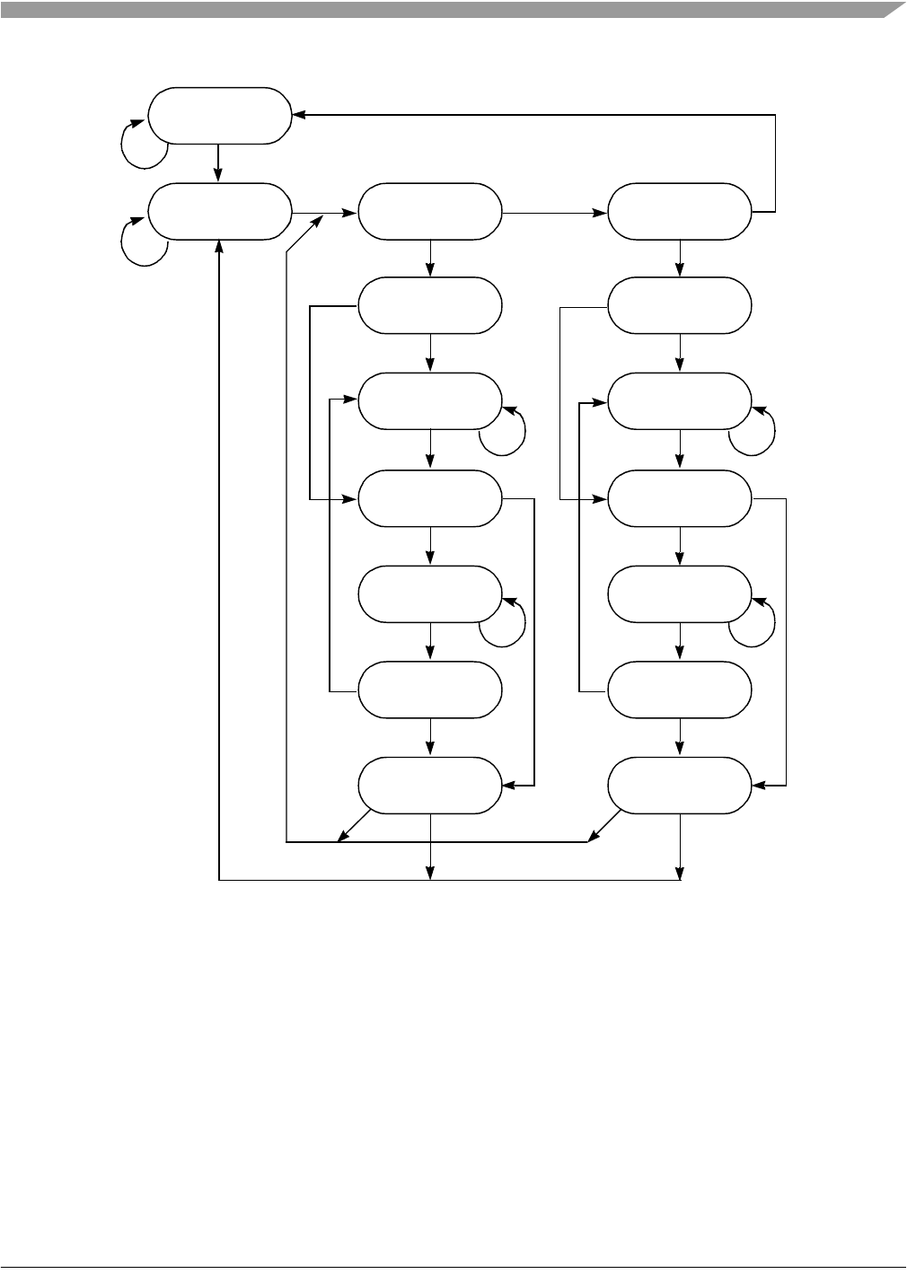
30.5.1.3 ABR Flowcharts
Figure 30-11. ABR Transmit Flow
Figure 30-12. ABR Transmit Flow (Continued)
Figure 30-13. ABR Transmit Flow (Continued)
Figure 30-14. ABR Receive Flow
30.5.2 RM Cell Structure
30.5.2.1 RM Cell Rate Representation
Figure 30-16. Rate Formula for RM Cells
Table30-7. Fields and th eir Positions in RM Cells
Figure 30-15. Rate Format for RM Cells
30.5.3 ABR Flow Control Setup
30.6 OAM Support
30.6.1 ATM-Layer OAM Definitions
30.6.2 Virtual Path (F4) Flow Mechanism
30.6.3 Virtual Channel (F5) Flow Mechanism
30.6.4 Receiving OAM F4 or F5 Cells
30.6.5 Transmitting OAM F4 or F5 Cells
30.6.6 Performance Monitoring
30.6.6.1 Running a Performance Block Test
30.6.6.2 PM Block Monitoring
30.6.6.3 PM Block Generation
30.6.6.4 BRC Performance Calculations
30.7 User-Defined Cells (UDC)
30.7.1 UDC Extended Address Mode (UEAD)
30.8 ATM Layer Statistics
30.9 ATM-to-TDM Interworking
30.9.1 Automatic Data Forwa rding
30.9.2 Using Interrupts in Automatic Data Forwarding
30.9.3 Timing Issues
30.9.4 Clock Synchronization (SRTS and Adaptive FIFOs)
30.9.5 Mapping TDM Time Sl ots to VCs
30.9.6 CAS Support
30.9.7 Trunk Condition
30.10 ATM Memory Structure
30.10.1 Parameter RA M
Page
Page
30.10.1.1 Determining UEAD_OFFSET (UEAD Mode Only)
30.10.1.2 VCI Filtering (VCIF)
Table30-12. UEAD_OFF SETs for Extended Addresses in the UDC Extra Header
Figure 30-22. VCI Filtering Enable Bits Table30-13. VCI F iltering Enable Field Descriptions
30.10.1.3 Global Mode Entry (GMODE)
Figure 30-23 shows the layout of the global mode entry (GMODE).
Table30-14 describes GMODE fields.
Figure 30-23. Global Mode Entry (GMODE) Table30-14. GMODE Field Descri ptions
30.10.2 Connection Tables (RCT, TCT, and TCTE)
30.10.2.1 ATM Channel Code
30.10.2.2 Receive Connection Table (RCT)
Table30-16 describes RCT fields.
Figure 30-25. Receive Connection Table (RCT) Entry
Table30-16. RCT Field Descriptions
Table30-16. RCT Field Descriptions (continued)
Table30-17 describes AAL 5 protocol specific RCT fields.
Figure 30-26. AAL5 Protocol-Specific RCT Table30-17. RCT Settings (AAL5 Protocol-Specific)
Table30-18 describes AAL5-ABR protocol-specific RCT fields.
Figure 30-28. AAL1 Protocol-Specif ic RCT
Table30-19 describes AAL 1 protocol-specific RCT fields.
Table30-19. AAL1 Protocol-Specific RCT Field Descriptions
Table30-20 describes AAL 0 protocol specific RCT fields.
Figure 30-29. AAL0 Protocol-Specif ic RCT Table30-20. AAL0-Specific RCT Field Descriptions
Table30-19. AAL1 Protocol-Specific RCT Field Descriptions (continued)
30.10.2.3 Transmit Connection Table (TCT)
Figure 30-30. Transmit Connection Table (TCT) Entry
Figure 30-30 shows the format of an TCT entry.
Table30-20. AAL0-Specific RCT Field Descriptions (continued)
Page
Page
Table30-21. TCT Field Descriptions
Table30-21. TCT Field Descriptions (continued)
30.10.2.3.1 AAL5 Protocol-Specific TCT Figure 30-31 shows the AAL5 protocol-specific TCT.
Table30-22 describes AAL 5 protocol-specific TCT fields.
30.10.2.3.2 AAL1 Protocol-Specific TCT Figure 30-32 shows the AAL1 protocol-specific TCT.
Figure30-31. AAL5 Protocol-Specific TCT Table30-22. AAL5-Specific T CT Field Descriptions
Table30-21. TCT Field Descriptions (continued)
Table30-23 describes AAL 1 protocol-specific TCT fields.
Figure30-32. AAL1 Protocol-Specific TCT Table30 -23. AAL1 Protocol-Specific TCT Field Des criptions
Page
Table30-25 describes VBR protocol-specific TCTE fields.
30.10.2.3.7 UBR+ Protocol-Specific TCTE Figure 30-35 shows the UBR+ protocol-specific TCTE.
Table30-26 describes UBR+ protocol-specific TCTE fields.
30.10.2.3.8 ABR Protocol-Specific TCTE Figure 30-36 shows the ABR protocol-specific TCTE.
Table30-27 describes ABR -specific TCTE fields.
Figure 30-36. ABR Protocol-Specific TCTE Table30-27. ABR-Specific TCTE Field Desc riptions
Table30-27. ABR-Specific TCTE Field Desc riptions (continued)
30.10.3 OAM Performance Monitoring Tables
30.10.4 APC Data Structure
Table30 -28. OAMPerformance Monitoring Table Field D escriptions
Figure 30-38. ATM Pace Control Data Structure
30.10.4.1 APC Parameter Tables
Table30-29. APC Parameter Table
30.10.4.2 APC Priority Table
Slot N+1 is used as a control slot, as shown in Figure30-40.
30.10.4.3 APC Scheduling Tables
Figure30-39. The APC Scheduling Table Structure
Table30-30. APC Priority Table Entry
30.10.5 ATM Controller Buffer Descriptors (BDs)
30.10.5.1 Transmit Buffer Operation
30.10.5.2 Receive Buffer Operation
Page
Figure 30-43. Receive Global Buffer Allocation Example
Figure 30-44. Free Buffer Pool Structure
Figure 30-45 describes the structure of a free buffer pool entry.
Table30-32 describes free buffer pool entr y fields.
Figure 30-45. Free Buffer Pool Entry Table30-32. Free Buffer Pool Entry Field Descriptions
Table30-33. Free Buffer Pool Parameter Table
30.10.5.3 ATM Controller Buffers
Table30-34 describes properties of the ATM receive and transmit buffers.
Figure 30-46. AAL5 RxBD
Figure 30-46 shows the AAL5 RxBD.
30.10.5.4 AAL5 RxBD
Table30-35 describes AAL 5 RxBD fields.
30.10.5.5 AAL1 RxBD
Figure 30-47 shows the AAL1 RxBD.
Figure 30-47. AAL1 RxBD
Table30-36 describes AAL 1 RxBD fields.
Table30-35. AAL5 RxBD Field Descriptions (continued)
30.10.5.6 AAL0 RxBD
Figure 30-48 shows the AAL0 RxBD.
Figure 30-48. AAL0 RxBD
Table30-37 describes AAL 0 RxBD fields.
Table30-36. AAL1 RxBD Field Descriptions
30.10.5.7 AAL1 CES RxBD
Refer to Section 31.12.1, AAL1 CES RxBD.
Refer to Section 32.4.4.4, CPS Receive Buffer Descriptor (RxBD).
30.10.5.8 AAL2 RxBD
Table30-37. AAL0 RxBD Field Descriptions
30.10.5.9 AAL5, AAL1 CES User-Defined CellRxBD Extension
30.10.5.10 AAL5 TxBDs
30.10.5.11 AAL1 TxBDs
Figure 30-51 shows the AAL1 TxBD.
Table30-38. AAL5 TxBD Field Descriptions
Table30-39 describes AAL 1 TxBD fields.
30.10.5.12 AAL0 TxBDs
Figure 30-51. AAL1 TxBD Table30-39. AAL1 TxBD Field Descriptions
Table30-40 describes AAL 0 TxBD fields.
30.10.5.13 AAL1 CES TxBDs
Refer to Section 31.12.2, AAL1 CES TxBDs
Figure 30-52. AAL0 TxBDs Table30-40. AAL0 TxBD Field Descriptions
30.10.5.14 AAL2 TxBDs
30.10.5.15 AAL5, AAL1 User-Defined CellTxBD Extension
30.10.6 AAL1 Sequence Number (SN) P rotection Table
30.10.7 UNI Statistics Table
30.11 ATM Exceptions
30.11.1 Interrupt Queues
30.11.2 Interrupt Queue Entry
30.11.3 Interrupt Queue Parameter Tables
Table30-42. Interrupt Queue Entry Field Description
Table30-43. I nterrupt Queue Parameter Table
30.12 The UTOPIA Interface
Table30-44 describes UTOPIA master mode signals.
30.12.1 UTOPIA Interface Master Mode
Figure 30-57. UTOPIA Master Mode Signals
Table30-44. UTOPIA Master Mode Signal Descriptions
30.12.1.1 UTOPIA Master Multiple PHY Operation
Table30-44. UTOPIA Master Mode Signal Descriptions (continued)
30.12.2 UTOPIA Interface Slave Mode
Figure 30-58. UTOPIA Slave Mode Signals
Table30-45 describes UTOPIA slave mode signals.
Table30-45. UTOPIA Slave Mod e Signals
30.12.2.1 UTOPIA Slave Multiple PHY Operation
30.13 ATM Registers
30.13.1 General FCC Mode Register (GFMR)
Table30-47 describes FPSMR fields.
30.13.2 FCC Protocol-Specific Mode Register (FPSMR)
Figure 30-59. FCC ATM Mode Register (FPSMR) Table30-47. FCC ATM Mode Register (FPSMR)
Table3 0-47. FCC ATM Mode Register (FPSM R) (continued)
30.13.3 ATM Event Register (FCCE)/Mask Register (FCCM)
Table3 0-47. FCC ATM Mode Register (FPSM R) (continued)
Table30-48 describes FCCE fields.
30.13.4 FCC Transmit Internal Rate Registers (FTIRR
(FCC1 and FCC2 Only)
Page
30.14 ATM Transmit Command
30.15 SRTS Generation and Clock Recovery Using External Logic
30.16 Configuring the ATM Controller for Maximum CPM Performance
30.16.1 Using Transmit Internal Rate Mode
30.16.2 APC Configuration
30.16.3 Buffer Configuration
Chapter 31 ATM AAL1 Circuit Emulation Service
31.1 Features
Page
31.2 AAL1 CES Transmitter Overview
31.2.1 Data Path
31.2.2 Signalin g Path
31.3 AAL1 CES Receiver Overview
Page
31.4 Interworking Functions
Multiplexing low speed services, such as voice and data, onto one ATM connection
31.4.1 Automatic Data Forwarding
31.4.1.1 ATM-to-TDM
31.4.1.2 TDM-to-ATM
31.4.2 Timing Issues
31.4.3 Clock Synchronization (SRTS, Adaptive FIFO)
31.4.4 Mapping TDM Time Slots to VCs
31.4.5 Trunk Condition
31.4.6 Channel Associated Signaling (CAS) Suppor t
Figure 31-8. Internal CAS Block Formats 31.4.7 Mapping VC Signaling to CAS Blocks
Figure 31-9. Mapping CAS Entry
31.4.7.1 CAS Routing Table
Figure 31-11. AAL1 CES CAS Routing Table Entry
Figure 31-10. AAL1 CES CAS Routing Table (CRT)
Figure 31-11 describes the structure of a CAS routing table entry.
31.4.7.2 TDM-to-ATM CAS Support
31.4.7.3 ATM-to-TDM CAS Support
31.5 ATM-to-TDM Adaptive Slip Control
31.5.1 CES Adaptive Threshold Tables
Table31-2 describes CES ada ptive threshold table fields.
Figure 31-16. Pre-Underrun Sequence
Figure 31-17. Pre-Overrun Sequence
31.6 3-Step-SN Algorithm
31.6.1 The Three St ates of the Algorithm
31.7 Pointer Verification Mechanism
31.8 AAL-1 Memory Structure
31.8.1 AAL1 CES Parameter RAM
Page
Table31-3. AAL1 C ES Field Descriptions (continued)
Additional CES parameters needed by the AAL1 microcode are described in the following table.
31.9 Receive and Transmit Connection Tables (RCT, TCT)
Table31-4. AAL1 CES Parameters
31.9.1 Receive Connection Table (RCT)
Table31 -5. RCT Field Descriptions
31.9.1.1 AAL1 CES Protocol-Specific RCT
Figure 31-22 shows the AAL1 CES protocol-specific area of an RCT entry.
Figure 31-22. AAL1 CES Protoc ol-Specific RCT
Table31-5. RCT Field Descriptions (continued)
Table31-6 describes AAL1 C ES protocol-specific RCT fields.
Figure 31-22. AAL1 CES Protoc ol-Specific RCT
Table31-6. AAL1 CES Protocol-Specific RCT Field Descriptions
Table31-6. AAL1 CES Protocol-Specific RCT Field Descriptions (continued)
31.9.2 Transmit Connection Table (TCT)
Figure 31-23 shows the format of an TCT entry.
Figure 31-23. Transmit Connection Table (TCT) Entry
Table31-7 describes general TCT fields.
Table31-7. TCT Field Descriptions
Table31-7. TCT Field Descriptions (continued)
31.9.2.1 AAL1 CES Protocol-Specific TCT
Figure 31-24 shows the AAL1 CES protocol-specific transmission connection tables (TCT).
Table31-8 describes AAL1 C ES protocol-specific TCT fields.
31.10 Outgoing CAS Status Register (OCASSR)
Figure31-25. Outgoing CAS Status Register (OCASSR)
Table31-9. OC ASSR Field Descriptions
Table31 -8. AAL1 CES Protocol-Specific TCT Field Des criptions (continued)
31.11 Buffer Descriptors
31.11.1 Transmit Buffer Operation
Figure 31-26. Transmit Buffers and BD Table Example
31.11.2 Receive Buffer Operation
Figure 31-27. Receive Buffers and BD Table Example
31.12 ATM Controller Buffers
Table31-10 describes properties of the ATM receive and transmit buffers.
Figure 31-28 shows the AAL1 CES RxBD.
31.12.1 AAL1 CES RxBD
Table31-10. Receive an d Transmit Buffers
Table31-11 describes AAL1 CES RxBD fields.
Figure 31-28. AAL1 CES RxBD Table31-11. AAL1 CES RxBD Field Descriptions
31.12.2 AAL1 CES TxBDs
Figure 31-29 shows the AAL1 CES TxBD.
Table31-12 describes AAL1 C ES TxBD fields.
Figure 31-29. AAL1 CES TxBD Table31-12. AAL1 CES TxBD Field Descriptions
31.13 AAL1 CES Exceptions
31.13.1 AAL1 CES Interrupt Queue Entry
31.14 AAL1 Sequence Number (SN) Protection Table
Table31-13. AAL1 CES Interrupt Queue Entr y Field Descriptions (continued)
31.15 Internal AAL1 CES Statistics Tables
Figure 31-31. AAL1 Sequence Number (SN) Protection Table
Table31-14. AAL1 CES DPR Statistics Table
31.16 External AAL1 CES Statistics Tables
31.17 CES-Specific Additions to the MCC
31.18 Application Considerations
Page
Page
Chapter 32 ATM AAL2
32.1 Introduction
Page
X
32.2 Features
Page
32.3 AAL2 Transmitter
32.3.1 Transmitter Overview
32.3.2 Transmit Priority Mechanism
32.3.2.1 Round Robin Priority
32.3.2.2 Fixed Priority
32.3.3 Partial Fill Mode (PFM)
32.3.4 No STF Mode
32.3.5 AAL2 Tx Data Structures
32.3.5.1 AAL2 Protocol-Specific TCT
Page
Page
Page
32.3.5.2 CPS Tx Queue Descriptor
Table32-2 describes the CPS TxQD fields. .
Figure 32-7. CPS Tx Queue Descriptor (TxQD) Table32-2. CPS TxQD Field Descriptions
32.3.5.3 CPS Buffer Structure
Figure 32-9 shows a CPS TxBD.
Figure 32-8. Buffer Structure Example for CPS Packets
Table32-2. CPS TxQD Field Descriptions (continued)
Table32-3 describes the CPS TxBD fields.
Figure 32-9. CPS TxBD Table32-3. CPS TxBD Field Descriptions
32.3.5.4 SSSAR Tx Queue Descriptor
.
32.3.5.5 SSSAR Transmit Buffer Descriptor
Figure 32-12. SSSAR TxBD Table32-5. SSSAR T xBD Field Descriptions
32.4 AAL2 Receiver
32.4.1 Receiver Overview
32.4.2 Mapping of PHY | VP | VC | CID
32.4.3 AAL2 Switching
32.4.4 AAL2 RX Data Structures
32.4.4.1 AAL2 Protocol-Specific RCT
Page
Table32-6. AAL2 Protocol-Specific RCT Field Descriptions
32.4.4.2 CID Mapping Tables and RxQDs
32.4.4.3 CPS Rx Queue Descriptors
32.4.4.4 CPS Receive Buffer Descriptor (RxBD)
Figure 32-17. CPS Receive Buffer Descriptor
Table32-8 describes the CPS RxBD fields.
Table32-7. CPS RxQD Field Descriptions
32.4.4.5 CPS Switch Rx Queue Descriptor
The switch RxQD, shown in Figure32-18, is used for CIDs that are being switched from one PHY1|VP
2|CID
2|VC
1 to another PHY2|VP
32.4.4.6 SWITCH Receive/Transmit Buffer Descriptor (RxBD)
Figure 32-19. Switch Receive/Transmit Buffer Descriptor
Table 3-11 describes the Switch RxBD fields.
Figure 32-18. CPS Switch Rx Queue Descriptor Table32-9. CPS Switch RxQD Field Descriptions
32.4.4.7 SSSAR Rx Queue Descriptor
Table32-10. Switch RxBD Field Descriptions
Table32-11 describes the SSSAR RxQD fields.
Figure 32-20. SSSAR Rx Queue Descriptor Table32-11. SSSAR Rx QD Field Descriptions
32.4.4.8 SSSAR Receive Buffer Descriptor
Figure 32-21. SSSAR Receive Buffer Descriptor
Table32-12 describes the SSSAR RxBD fields.
Table32-11. SS SAR RxQD Field Descriptions (continued)
Table32-12. SSSAR R xBD Field Descriptions
32.5 AAL2 Parameter RAM
Table32-13. AAL2 Parameter RAM
.
Table32-13. AAL2 Parameter RAM (continued)
32.6 User-Defined Cells in AAL2
32.7 AAL2 Exceptions
Table32-14 describes the interrupt queue entry fields for a CID.
An interrupt entry for the VC is shown in Figure 32-24.
Figure 32-24. AAL2 Interrupt Queue Entry CID = 0
Table32-15. AAL2 Inter rupt Queue Entry CID = 0 Field Descriptions
Page
Page
33.1.1 References
33.1.2 IMA Versions Supported
33.1.3 PowerQUICC II Versions Supported
33.1.4 PHY-Layer Devices Suppor ted
33.1.5 ATM Features Not Supported
33.2 IMA Protocol Overview
33.2.1 Introduction
33.2.2 IMA Frame Overview
Page
33.2.3 Overview of IMA Cells
33.2.3.1 IMA Control Cells
Page
Page
Figure 33-4. IMA Frame and ICP Cell Formats
33.2.3.2 IMA Filler Cells
33.3 IMA Microcode Architecture
This chapter explains the architecture of the receive and transmit IMA microcode tasks.
33.3.1 IMA Function Partitioning
IMA Frame
33.3.1.1 User Plane Functions Performed by Microcode
33.3.2 Transmit Architecture
33.3.2.1 TRL Operation
33.3.2.2 Non-TRL Operation
33.3.2.3 Transmit Queue Operation Examples (ITC mode)
Figure 33-8. Transmit Queue Behavior: Link Clock Rate Slower than TRL
Figure 33-9. Transmit Queue Behavior: Link Clock Rate Faster than TRL, Worst-Case Event Sequence
33.3.2.4 Differences in CTC Operation
is held off for minimum
33.3.3 Receive Architecture
33.3.3.1 Cell Reception Task
Page
Cell Reception Task
Configuration to reach to move to next state
No Link Defect
- According to the Links state, the Microcode executes dif ferent Tasks
- Each IMA Link follows a Four-State Ma chine
Page
Page
33.3.3.2 Cell Processing Activation Function
Page
33.3.3.3 Cell Processing Task
33.4 IMA Programming Model
33.4.1 Data Structure Organ ization
Page
33.4.2 IMA FCC Programming
33.4.2.1 FCC Registers
33.4.2.2 FCC Parameters
33.4.2.3 IMA-Specific FCC Parameters
IMAROOT must be programmed to a 128-byte aligned address terminating with 0x80 (i.e. 0xnn80).
33.4.3 IMA Root Table
Table33 -3. IMA Root Table1 (continued)
33.4.3.1 IMA Control (IMACNTL)
33.4.4 IMA Group Tables
33.4.4.1 IMA Group Transmit Table Entry
Table33-5. IMA Group Transmit Table Entry
Figure 33-14. IMA Group Transmit Control (IGTCNTL) Table33-6. IGTCNTL Field Descriptions
Table33-5. IMA Group Transmit Table Entry (continued)
Page
Page
Table 33-9. ICP Cell Tem plate (continued)
parameters are managed by the microcode and should be initialized to zero unless otherwise stated.
Table 33-9. ICP Cell Tem plate (continued)
33.4.4.2 IMA Group Receive Table Entry
Table33-10. IMA Group Receive Table Entry
Table33-10. IMA Group Re ceive Table Entry (continued)
Figure 33-17. IMA Group Receive Control (IGRCNTL)
Table33-10. IMA Group Re ceive Table Entry (continued)
33.4.4.2.3 IMA Receive Group Frame Size The fields of the IRGFS register are shown in Figure33-19.
Table33-11. IGRCNTL Field Descriptions
Figure 33-18. IMA Group Receive State (IGRSTATE) Table33-12. IGRSTATE Field Descriptions
Page
33.4.5 IMA Link Tables
33.4.5.1 IMA Link Transmit Table Entry
Table33-14. R eceive Group Order Table Entry Field Descriptions
Table33-15. IMA Link Transmit Table Entry
Figure 33-21. IMA Link Transmit Control (ILTCNTL) Table33-16. ILTCNTL Field Descriptions
Table33 -15. IMA Link Transmit Table Entry (con tinued)
Figure 33-23. IMA Transmit Interrupt Status (ITINTSTAT)
Figure 33-22. IMA Link Transmit State (ILTSTATE) Table33-17. ILTSTATE Field Descriptions
Table33-16. ILTCNTL Field Descriptions (continued)
Table33-18 describes the ITINTSTAT bit fields.
33.4.5.2 IMA Link Receive Table Entry
Table33-18. ITINTSTAT Field Descriptions
Table33 -19. IMA Link Receive Table Entry
Table33 -19. IMA Link Receive Table Entry1 (continued)
Table33-20 describes the ILRCNTL bit fields.
Figure 33-24. IMA Link Receive Control (ILRCNTL) Table33-20. ILRCNTL Field Descriptions
Table33-21 describes the ILRSTATE bit fields.
Figure 33-25. IMA Link Receive State (ILRSTATE) Table33-21. ILRSTATE Field Descriptions
33.4.5.3 IMA Link Receive Statistics Table
33.4.6 Structures in External Memory
33.4.6.1 Transmit Queues
33.4.6.2 Delay Compensation Buffers (DCB)
33.4.7 IMA Exceptions
33.4.7.1 IMA Interrupt Queue Entry
33.4.7.2 ICP Cell Reception Exceptions
Table33-23. IMA I nterrupt Queue Entry Field Descriptions
33.4.8 IDCR Timer Programming
33.4.8.1 IDCR Master Clock
33.4.8.2 IDCR FCC Parameter Shadow
Page
33.4.8.3 IDCR_Init Command
33.4.8.4 IDCR Root Parameters
33.4.8.5 IDCR Table Entry
33.4.8.6 IDCR Counter Algorithm
33.4.8.7 IDCR Events
33.4.9 APC Programming for IMA
33.4.9.1 Programming for CBR, UBR, VBR, and UBR+
33.4.9.2 Programming for ABR
33.4.10 Changing IMA Version
33.5 IMA Software Interface and Requirements
33.5.1 Software M odel
33.5.2 Initialization Procedure
33.5.3 Software Responsibilities
33.5.3.1 System Definition
33.5.3.2 General Operation
33.5.3.3 Receive Link State Machine Control
33.5.3.4 Receive Group State Machine Control
33.5.3.5 Transmit Link State Machine Control
33.5.3.6 Transmit Group State Machine Control
33.5.3.7 Group Symmetry Control
33.5.3.8 ICP End-to-End Channel Transmission
33.5.3.9 Link Addition and Slow Recovery (LASR) Procedure
33.5.3.10 Failure Alarms
33.5.4 IMA Software Procedures
33.5.4.1 Transmit ICP Cell Signalling
33.5.4.2 Receive Link Start-up Procedure
33.5.4.3 Group Start-up Procedure
Page
33.5.4.4 Link Addition Procedure
Page
33.5.4.5 Link Removal Procedure
33.5.4.6 Link Receive Deactivation Procedure
33.5.4.7 Link Receive Reactivation Procedure
33.5.4.8 TRL On-the-Fly Change Procedure
33.5.4.9 Transmit Event Response Procedures
33.5.4.10 Receive Event Response Procedures
Page
33.5.4.11 Test Pattern Procedure
33.5.4.12 IDCR Operation
33.5.4.13 End-to-End Channel Signalling Procedure
Page
Page
Chapter 34 ATM Transmission Convergence Layer
34.1 Features
Page
34.2 Functionality
34.2.1 Receive ATM Cell Functions
Page
34.2.1.1 Receive ATM 2-Cell FIFO
34.2.2 Transmit ATM Cell Functions
34.2.2.1 Transmit ATM 2-Cell FIFO
34.2.3 Receive UTOPIA Interface
34.2.4 Transmit UTOPIA Interface
34.4.1.1 TC Layer Mode Register [18] (TCMODE
34.3 Signals
34.4 TC Layer Programming Mode
34.4.1 TC Layer Registers
)
Table34-2 describes TCMODE fields.
Figure 34-5. TC Layer Mode Register (TCMODEx) Table34-2. TCMO DEx Field Descriptions
34.4.1.2 Cell Delineation State Machine Register [18] (CDSMR
Table34-3. CDSMR
Figure 34-6. Cell Delineation State Machine Register (CDSMR
Table34-3 describes CDSMR fields.
Field Descriptions
34.4.1.3 TC Layer Event Register [18] (TCERx)
Figure 34-7. TC Layer Event Register (TCER
The TCER bits are described in Table 34-4.
Table34-4. TCER
Field Descriptions
34.4.2 TC Layer General Registers
34.4.2.1 TC Layer General Event Register (TCGER)
34.4.2.2 TC Layer General Status Register (TCGSR)
34.4.3 TC Layer Cell Counters
34.4.3.6 Filtered Cell Counter [18] (TC_FCC
34.4.4 Programming FCC2
34.4.5 Programming and Operating the TC Layer
34.4.5.1 Receive
34.4.5.2 Transmit
Page
34.5 Implementation Example
34.5.1 Operating the TC Layer at Higher Frequen cies
34.5.2 Programming a T1 Application
Step 1
Step 2
Step 3
Step 4
Step 5
Step 6
Step 7
Chapter 35 Fast Ethernet Controller
35.1 Fast Ethernet on the PowerQUICCII
35.2 Features
Page
35.3 Connecting the PowerQUICCII to Fast Ethernet
35.4 Ethernet Channel Frame Transmission
35.5 Ethernet Channel Frame Reception
35.6 Flow Control
35.7 CAM Interface
35.8 Ethernet Parameter RAM
For Ethernet mode, the protocol-specific area of the FCC parameter RAM is mapped as in Table35-2.
Table35-2. Ethernet-Specific Parameter RAM
Page
Page
35.9 Programming Model
The transmit and receive commands are issued to the CPCR; see Section14.4, Command Set.
35.10 Ethernet Command Set
Receive commands that apply to Ethernet are described in Table 35-4.
Table35-3. Transmit Commands
Table35-4. Receive Commands
35.11 RMON Support
35.12 Ethernet Address Recognition
Table35 -5. RMON Statistics and Counters (continued)
Page
35.13 Hash Table Algorithm
35.14 Interpacket Gap Time
35.15 Handling Collisions
35.16 Internal and External Loopback
35.17 Ethernet Error-Handling Procedure
Transmission errors are described in Table35-6.
35.18 Fast Ethernet Registers
35.18.1 FCC Ethernet Mode Register (FPSMR)
Table35-6. Transmission Errors
Table35 -7. Reception Errors
Table35-8 describes FPSMR fields.
Figure 35-5. FCC Ethernet Mode Registers (FPSMR) Table35-8. FPSMR Ethernet Field Descriptions
35.18.2 Ethernet Event Register (F CCE)/Mask Register (FCCM)
Figure 35-6. Ethernet Even t Register (FCCE)/Mask Regist er (FCCM)
Table35-8. FPSMR Ethernet Field Descriptions (continued)
Table35-9 describes FCCE/FCCM fields.
Figure 35-6. Ethernet Even t Register (FCCE)/Mask Regist er (FCCM)
Figure 35-7 shows interrupts that can be generated in the Ethernet protocol.
Table35-9. FCCE/FCCM Field Descriptions
Figure 35-7. Ethernet Interrupt Events Example
35.19 Ethernet RxBDs
Table35-10 describes Ethernet RxBD fields.
Figure 35-8. Fast Ethernet Receive Buffer (RxBD) Table35-10. RxBD Field Descriptions
Page
Figure 35-9. Ethernet Receiving Using RxBDs
35.20 Ethernet TxBDs
Table35-11 describes Ethernet TxBD fields .
Figure 35-10. Fast Ethernet Transmit Buffer (TxBD) Table35-11. Ethernet TxBD Field Definitions
Page
Page
Chapter 36 FCC HDLC Controller
36.1 Key Features
36.2 HDLC Channel Frame Transmission Processing
36.3 HDLC Channel Frame Reception Processing
36.4 HDLC Parameter RAM
Figure 36-2 shows an example of using HMASK and HADDR[14].
Table36 -1. FCC HDLC-Specific Parameter RAM Memory Map (continued)
Figure 36-2. HDLC Address Re cognition Example
36.5 Programming Model
36.5.1 HDLC Command Set
Table36-2. Transmit Commands
Table36-3 describes the receive commands that apply to the HDLC controller.
36.5.2 HDLC Error Handling
Table36-5 describes HDLC reception errors, which are reported through the RxBD.
Table36-3. Recei ve Commands
Table36-4. HDLC Transmission Errors
Table36-2. Transmit Commands (continued)
36.6 HDLC Mode Register (FPSMR)
Table36-5. HDLC Reception Errors
The FPSMR fields are described in Table36-6.
Figure 36-3. HDLC Mode Register (FPSMR) Table36 -6. FPSMR Field Descriptions
36.7 HDLC Receive Buffer Descriptor (RxBD)
Table36-6. FPSMR F ield Descriptions (continued)
Figure 36-4. FCC HDLC Receiving Using RxBDs
Figure 36-5 shows the FCC HDLC RxBD.
Table36-7 describes RxB D fields.
Figure 36-5. FCC HDLC Receive Buffer Descriptor (RxBD) Table36-7. RxBD field De scriptions
36.8 HDLC Transmit Buffer Descriptor (TxBD)
Table36-8. HDLC TxBD F ield Descriptions
36.9 HDLC Event Register (FCCE)/Mask Register (FCCM)
Figure 36-8 shows interrupts that can be generated in the HDLC protocol.
Table36-9. FCCE/FCCM Field Descriptions
Figure 36-8. HDLC Interrupt Event Example
36.10 FCC Status Register (FCCS)
Figure 36-9. FCC Status Register (FCCS)
Table36-10 describes FCCS bits.
Table36-10. FCCS Register Field Descriptions
Page
Chapter 37 FCC Transparent Controller
37.1 Features
37.2 Transparent Channel Operation
37.3 Achieving Synchronization in Transparent Mode
37.3.1 In-Line S ynchronization Pattern
37.3.2 External Synchronization Signals
37.3.3 Transparent Synchronization Ex ample
Figure 37-2. Sending Transparent Frames between PowerQUICCIIs
Chapter 38 Serial Peripheral Interface (SPI)
38.1 Features
38.2 SPI Clocking and Signal Functions
38.3 Configuring the SPI Controller
38.3.1 The SPI as a Master Device
38.3.2 The SPI as a Slave Device
38.3.3 The SPI in Multimaster Operation
Figure 38-3. Multimaster Configuration
38.4 Programming the SPI Registers
Table38-1 describes the SPMODE fields.
The following sections describe the registers used in configuring and operating the SPI.
38.4.1 SPI Mode Re gister (SPMODE)
Figure 38-4. SPMODESPI Mode Register Table38-1. SPMODE Field Descriptions
Figure 38-5. SPI Transfer Format with SPMODE[CP] = 0
Table38-1. SPMODE Field Descriptions (continued)
Figure 38-6. SPI Transfer Format with SPMODE[CP] = 1
38.4.1.1 SPI Examples with Different SPMODE[LEN] Values
Example 2
Example 1
Table38-2. Example Conventions
with REV=1, the string is byte reversed and transmitted, a byte at a time, with lsb first:
38.4.2 SPI Event/Mask Registers (SPIE/SPIM)
Table38-3 describes the SPIE/SPIM fields.
Figure 38-7. SPIE/SPIMSPI Event/Mask Registers Table38-3. SPIE/SPIM Field Descriptions
38.4.3 SPI Command Register (SPCOM)
38.5 SPI Parameter RAM
Table38-5. S PI Parameter RAM Memory Map
38.5.1 Receive/Transmit Function Code Registers (RFCR /TFCR)
Figure 38-9 shows the fields in the receive/transmit function code registers (RFCR/TFCR).
Table38-7 lists transmit/receive commands sent to the CP command register (CPCR).
Table38-6 describes the RFCR/TFCR fields.
38.6 SPI Commands
Figure 38-9. RFCR/TFCRFunction Code Registers Table38-6. RFCR/TFCR Field Descriptions
Table38-7. SPI Commands
38.7 The SPI Buffer Descriptor (BD) Table
38.7.1 SPI Buffer Descriptors (BDs)
38.7.1.1 SPI Receive BD (RxBD)
38.7.1.2 SPI Transmit BD (TxBD)
Table38-9 describes the TxBD status and control fields.
Figure 38-12. SPI TxBD Table38-9. SPI TxBD Status and Control Field Descriptions
Table38 -8. SPI RxBD Status and Control Field Descriptions (continu ed)
38.8 SPI Master Programming Example
38.9 SPI Slave Programmin g Example
38.10 Handling Interrupts in the SPI
Chapter 39 I2C Controller
39.1 Features
39.2 I2C Controller Clocking and Signal Functions
39.3 I2C Controller Transfers
39.3.1 I2C Master Write (Slave Read)
39.3.2 I2C Loopback Testing
39.3.3 I2C Master Read (Slave Write)
39.3.4 I2C Multi-Master Considerations
39.4 I2C Registers
The following sections describe the I2C registers.
The I2C address register, shown in Figure 39-7, holds the address for this I2C port.
39.4.1 I2C Mode Register (I2MOD)
The I2C mode register, shown in Figure39-6, controls the I2C modes and clock source.
39.4.3 I2C Baud Rate Generator Register (I2BRG)
The I2C baud rate generator register, shown in Figure 39-8, sets the divide ratio of the I2C BRG.
Table39-3 describes I2BRG fields.
39.4.4 I2C Event/Mask Registers (I2CER/I2CMR)
Figure 39-7. I2C Address Register (I2ADD) Table39-2. I2ADD Field Descr iptions
39.4.5 I2C Command Register (I2COM)
Table39-5 describes I2 COM fields.
Figure 39-9. I2C Event/Mask Registers (I2CER/I2CMR) Table39-4. I2CER/I2CMR Field Descriptions
Figure 39-10. I2C Command Register (I2COM) Table39-5. I2COM Field Descriptions
39.5 I2C Parameter RAM
Table39-6. I2C Parameter RAM Memory Map
Table39-5. I2COM Field Descriptions
Figure 39-11 shows the RFCR/TFCR bit fields.
Table39-7 describes the RFCR/TFCR bit fields.
Figure 39-11. I2C Function Code Registers (RFCR/TFCR) Table39-7. RFCR/TFCR Field Descriptions
Table39-6. I2C Parameter R AM Memory Map (continued)
39.6 I2C Commands
39.7 The I2C Buffer Descriptor (BD) Table
Table39-8. I2C Transmit/Receive Commands
Table39-7. RFCR/TFCR Field Descriptions
39.7.1 I2C Buffer Descriptors (BDs)
39.7.1.1 I2C Receive Buffer Descriptor (RxBD)
Table39-9 describes I2C RxBD status and control bits.
39.7.1.2 I2C Transmit Buffer Descriptor (TxBD)
Figure 39-13. I2C RxBD Table39-9. I2C RxBD Status and Control Bits
Table39-10 describes I2C TxBD status and control bits.
Figure 39-14. I2C TxBD Table39-10. I2C TxBD Status and Control Bits
Chapter 40 Parallel I/O Ports
40.1 Features
40.2 Port Registers
40.2.1 Port Open-Drain Registers (PODRAPODRD)
40.2.2 Port Data Registers (PDATAPDATD)
40.2.3 Port Data Direction Registers (PDIRAPDIRD)
The port data direction register(PDIR), shown in Figure40-3, is cleared at syst em res et.
Table40-2 describes PDIR fi elds.
Figure 40-2. Port Data Registers (PDATAPDATD)
Figure 40-3. Port Data Direction Register (PDIR) Table40-2. PDIR Field Descriptions
40.2.4 Port Pin Assignment Register (PPAR)
The port pin assignment register (PPAR) is cleared at system reset.
Figure 40-5 shows the port special options registers (PSORx).
Table40-2 describes PPARx fields.
40.2.5 Port Special Options Registers AD (PSORAPSOR D)
40.3 Port Block Diagram
Figure 40-5. Special Options Registers (PSORAPOSRD) Table40-4. PSOR
Field Descriptions
Figure 40-6. Port Functional Operation
40.4 Port Pins Functions
Each pin can operate as a general purpose I/O pin or as a dedicated input or output pin.
40.4.1 General Purpose I/O Pins
40.4.2 Dedicated Pins
40.5 Ports Tables
Figure 40-7. Primary and Secondary Option Programming
Table40-5. Port ADedicated Pin Assignment (PPARA = 1)
Page
Page
Table40-6 shows the port B pin assignments.
Table40-6. Port B Dedicated P in Assignment (PPARB = 1)
Table40-6. Port B Dedicated Pin Assignment (PPARB = 1) (continued)
Table40-7 shows the port C pin assignments.
Table40-7. Port C Dedicated P in Assignment (PPARC = 1)
Table40-6. Port B Dedicated Pin Assignment (PPARB = 1) (continued)
Page
Table40-7. Port C Dedicated Pin Assignment (PPARC = 1) (continued)
Table40-8 shows the port D pin assignments.
Table40-8. Port D Dedicated Pin Assignment (PPARD = 1)
Table40-8. Port D Dedicated Pi n Assignment (PPARD = 1) (continued)
40.6 Interrupts from Port C
Table40-8. Port D Dedicated Pi n Assignment (PPARD = 1) (continued)
Page
Appendix A Register Quick Reference Guide
This section provides a brief guide to the core registers.
Programming Environments Manual
A.1 PowerPC RegistersUser Registers
Tabl e A-2 lists SPRs defined by the PowerPC architecture implemented on the MPC8260.
Tabl e A-4 lists supervisor-level SPRs defined by the PowerPC architecture.
TableA-3. Supervisor-Level PowerPC Registers
TableA-4. Supervisor-Level PowerPC SPRs
A.3 MPC8260-Specific SPRs
TableA-5. MPC8260-Sp ecific Supervisor-Level SPRs
Page
Appendix B Reference Manual (R ev 1) Errata
NOTE
B.1 Document Errata
Page
Page
Page
Page
Page
Page
Page
Page
Page
33.3.2.1.1 TRL Service Latency
33.4.1.1, 33-29 Add the following two rows to the bottom of Table 33-5:
33.4.4.1.1, 33-29 Add ISIE to Figure 33-14 and Table 33-6, as shown in the following:
33.4.5.1.2, 33-40 Add LDC to Figure 33-22 and Table 33-17, as shown in the following:
33.4.4.1.2, 33-30 Add GTE and TRQS to Figure 33-15 and Table 33-7, as shown in the following:
33.4.10 Changing IMA Version
Page
Page
Page
Glossary of Terms and Abbreviations
A
B
C
See also
D
E
F
G
see
H
I
L
See
n
M
N
O
P
Q R
S
T
U
V
W
Page
Index
Numerics
A
Page
B
C
Page
Page
Page
D
E
F
G
H
I
Page
J
L
M
Page
N
O
P
Page
Page
R
Page
Page
Page
S
Page
Page
T
U