LSI Specification | MB86617A |
3.1. Block Diagram
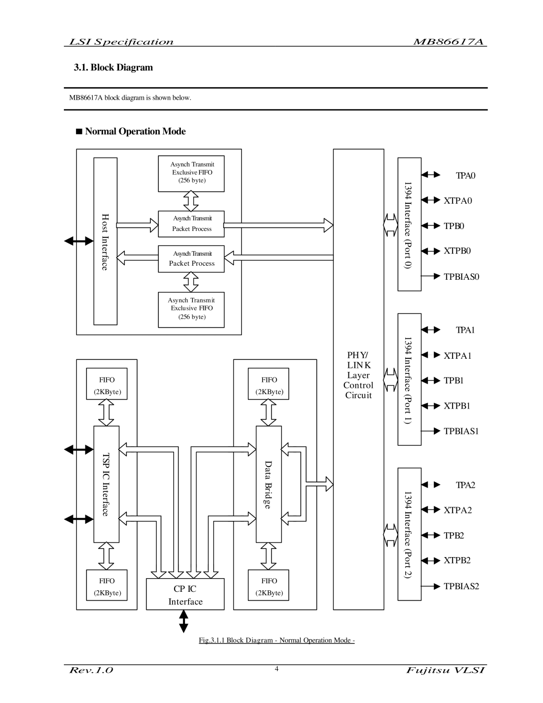
MB86617A block diagram is shown below.
<Normal Operation Mode
| Asynch Transmit |
| Exclusive FIFO |
| (256 byte) |
Host | Asynch Transmit |
Packet Process | |
Interface | Asynch Transmit |
Packet Process | |
| |
| Asynch Transmit |
| Exclusive FIFO |
| (256 byte) |
|
|
| PHY/ |
|
|
| LINK |
FIFO |
| FIFO | Layer |
| Control | ||
(2KByte) |
| (2KByte) | |
| Circuit | ||
TSP IC |
| Data |
|
Interface |
| Bridge |
|
FIFO | CP IC | FIFO |
|
(2KByte) | (2KByte) |
| |
Interface |
| ||
|
|
|
Fig.3.1.1 Block Diagram - Normal Operation Mode -
Rev.1.0 | 4 |
1394 |
| TPA0 |
| ||
| XTPA0 | |
Interface |
| |
| TPB0 | |
(Port0) |
| |
| XTPB0 | |
|
|
![]() TPBIAS0
TPBIAS0
1394 |
| TPA1 |
| ||
| XTPA1 | |
Interface |
| |
| TPB1 | |
(Port1) |
| |
| XTPB1 | |
|
|
![]() TPBIAS1
TPBIAS1
1394 |
| TPA2 |
| XTPA2 | |
Interface |
| |
| TPB2 | |
(Port2) |
| |
| XTPB2 | |
|
|
![]() TPBIAS2
TPBIAS2
Fujitsu VLSI