LSI Specification | MB86617A |
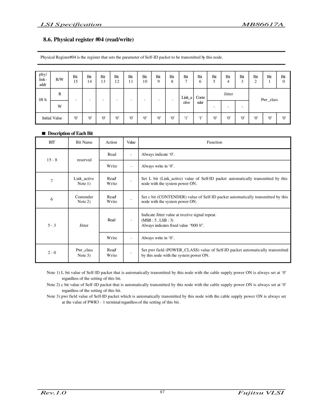
8.6. Physical register #04 (read/write)
Physical Register#04 is the register that sets the parameter of
phy/ |
| Bit | Bit | Bit | Bit | Bit | Bit | Bit | Bit | Bit | Bit | Bit | Bit | Bit | Bit |
| Bit |
| Bit |
link- | R/W |
|
| ||||||||||||||||
15 | 14 | 13 | 12 | 11 | 10 | 9 | 8 | 7 | 6 | 5 | 4 | 3 | 2 |
| 1 |
| 0 | ||
addr |
|
|
| ||||||||||||||||
|
|
|
|
|
|
|
|
|
|
|
|
|
|
|
|
|
|
| |
|
|
|
|
|
|
|
|
|
|
|
|
|
|
|
|
|
|
|
|
| R |
|
|
|
|
|
|
|
| Link_a | Conte |
| Jitter |
|
|
|
|
|
|
08 h |
| - | - | - | - | - | - | - | - |
|
|
|
| Pwr _class |
| ||||
| W |
|
|
|
|
|
|
|
| ctive | nder | - | - | - |
|
|
|
|
|
|
|
|
|
|
|
|
|
|
|
|
|
|
|
|
| ||||
|
|
|
|
|
|
|
|
|
|
|
|
|
|
|
|
|
|
| |
Initial Value | ‘0’ | ‘0’ | ‘0’ | ‘0’ | ‘0’ | ‘0’ | ‘0’ | ‘0’ | ‘1’ | ‘1’ | ‘0’ | ‘0’ | ‘0’ | ‘0’ |
| ‘0’ |
| ‘0’ | |
|
|
|
|
|
|
|
|
|
|
|
|
|
|
|
|
|
|
|
|
<Description of Each Bit
BIT | Bit Name | Action | Value | Function | |
|
|
|
|
| |
|
| Read | - | Always indicate ‘0’. | |
15 - 8 | reserved |
|
|
| |
Write | - | Always write in ‘0’. | |||
|
| ||||
|
|
|
|
| |
7 | Link_active | Read/ | - | Set L bit (Link_active) value of | |
Note 1) | Write | node with the system power ON. | |||
|
| ||||
|
|
|
|
| |
6 | Contender | Read/ | - | Set c bit (CONTENDER) value of | |
Note 2) | Write | node with the system power ON. | |||
|
| ||||
|
|
|
|
| |
|
|
|
| Indicate Jitter value at receive signal repeat. | |
|
| Read | - | (MSB : 5 , LSB : 3) | |
5 - 3 | Jitter |
|
| Always indicates fixed value “000 b”. | |
|
|
|
|
| |
|
| Write | - | Always write in ‘0’. | |
|
|
|
|
| |
2 - 0 | Pwr _class | Read/ | - | Set pwr field (POWER_CLASS) value of | |
Note 3) | Write | by this node with the system power ON. | |||
|
| ||||
|
|
|
|
|
Note 1) L bit value of
Note 2) c bit value of Self
Note 3) pwr field value of
Rev.1.0 | 87 | Fujitsu VLSI |
