LSI Specification | MB86617A |
8.5. Physical register #03 (read)
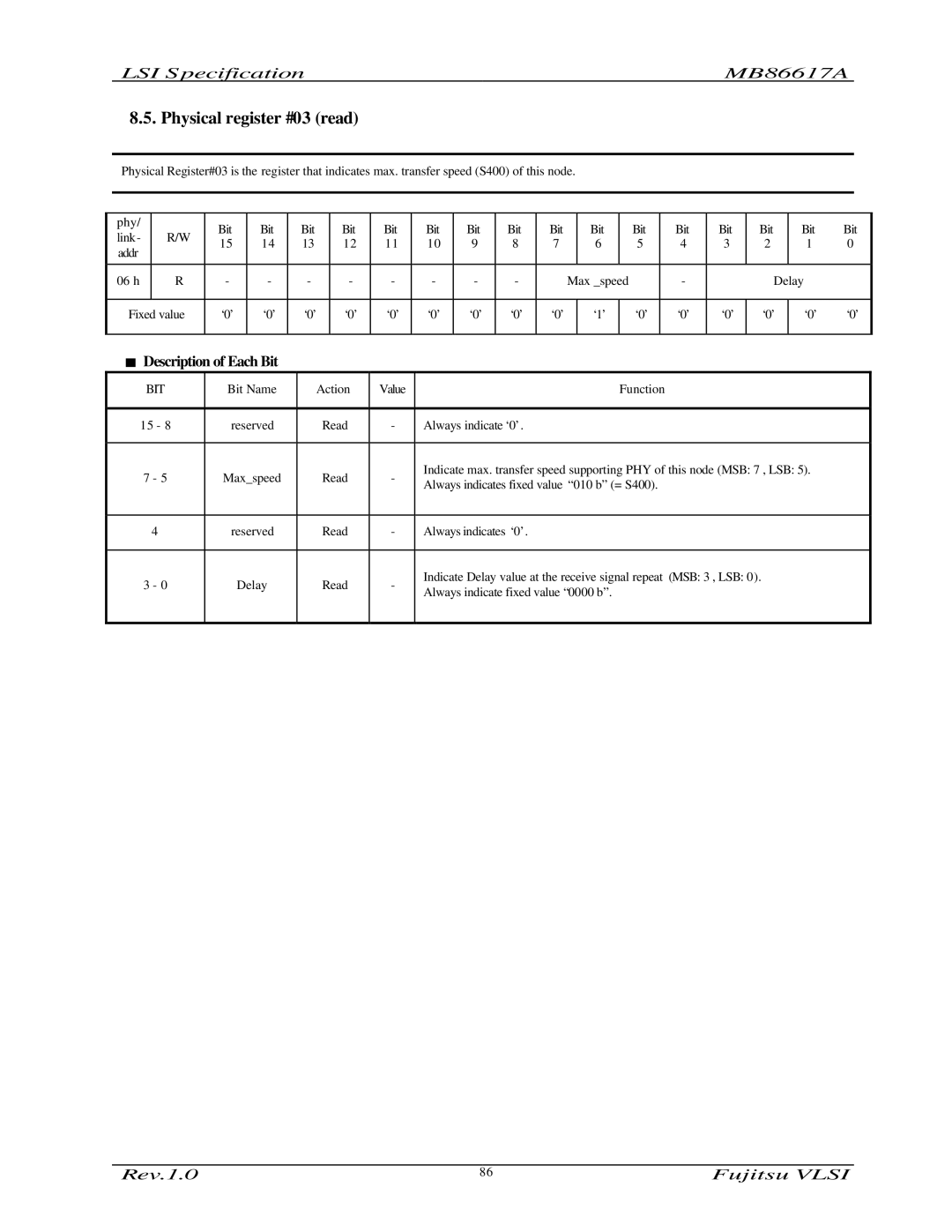
Physical Register#03 is the register that indicates max. transfer speed (S400) of this node.
phy/ |
| Bit | Bit | Bit | Bit | Bit | Bit | Bit | Bit | Bit |
| Bit |
| Bit | Bit | Bit | Bit | Bit | Bit |
link- | R/W |
|
| ||||||||||||||||
15 | 14 | 13 | 12 | 11 | 10 | 9 | 8 | 7 |
| 6 |
| 5 | 4 | 3 | 2 | 1 | 0 | ||
addr |
|
|
| ||||||||||||||||
|
|
|
|
|
|
|
|
|
|
|
|
|
|
|
|
|
|
| |
|
|
|
|
|
|
|
|
|
|
|
|
|
|
|
|
|
|
|
|
06 h | R | - | - | - | - | - | - | - | - |
| Max _speed |
| - |
| Delay |
| |||
|
|
|
|
|
|
|
|
|
|
|
|
|
|
|
|
|
|
| |
Fixed value | ‘0’ | ‘0’ | ‘0’ | ‘0’ | ‘0’ | ‘0’ | ‘0’ | ‘0’ | ‘0’ |
| ‘1’ |
| ‘0’ | ‘0’ | ‘0’ | ‘0’ | ‘0’ | ‘0’ | |
|
|
|
|
|
|
|
|
|
|
|
|
|
|
|
|
|
|
|
|
<Description of Each Bit
BIT | Bit Name | Action | Value | Function | |
|
|
|
|
| |
15 - 8 | reserved | Read | - | Always indicate ‘0’. | |
|
|
|
|
| |
7 - 5 | Max_speed | Read | - | Indicate max. transfer speed supporting PHY of this node (MSB: 7 , LSB: 5). | |
Always indicates fixed value “010 b” (= S400). | |||||
|
|
|
| ||
|
|
|
|
| |
4 | reserved | Read | - | Always indicates ‘0’. | |
|
|
|
|
| |
3 - 0 | Delay | Read | - | Indicate Delay value at the receive signal repeat (MSB: 3 , LSB: 0). | |
Always indicate fixed value “0000 b”. | |||||
|
|
|
| ||
|
|
|
|
|
Rev.1.0 | 86 | Fujitsu VLSI |
