Intel StrongARM SA-1100 Microprocessor
Developer’s Manual
SA-1100 Developer’s Manual
Contents
Caches, Write Buffer, and Read Buffer
Memory-Management Unit MMU
1.6
System Control Module
Reviving the DRAMs from Self-Refresh Mode
Memory and Pcmcia Control Module
Peripheral Control Module
11-39
11.8.3.4Endpoint 0 Interrupt Mask EIM 11-64 11.8.3.5Receive
11-81
SA-1100 Developer’s Manual
11-128
Serial Port 4 MCP / SSP
11-169
11.12.12.1Transmit Fifo Not Full Flag TNF
Register Summary MHz Oscillator Specifications
KHz Oscillator Specifications
Internal Test
Figures
SA-1100 Power and Clock Supply Sources and States
Tables
14-4
Page
LCD
Introduction
Intel StrongARM SA-1100 Microprocessor
DMA
Features of the SA-1100 CPU for AA and EA Parts
Features of the SA-1100 CPU for CA and DA Parts
Additional Features Built into SA-1100 Chipset
Changes to the SA-1100 Core from the SA-110
Overview
Example System
SA-1100 Example System
ARM Architecture
Write Buffer
Read Buffer
Page
Block Diagram
Functional Description
SA-1100 Block Diagram
Inputs/Outputs
Signal Description
Signal Descriptions Sheet 1
Name Type Description
Signal Descriptions Sheet 2
VDD
Signal Descriptions Sheet 3
TDO OCZ
VSS
Memory Map
1GB
Pcmcia Interface Mbyte Static Memory ROM, Flash, Sram
ARM Implementation Options
Big and Little Endian
Exceptions
Power-Up Reset
ROM Size Select
Abort
Exception Priorities
Address Exception Mode on Entry
Vector Summary
Vector Summary
Interrupt Latencies and Enable Timing
Coprocessors
Page
Instruction Set
Instruction Group Result Delay Issue Cycles
Instruction Set
Instruction Timings
Page
Coprocessors
Internal Coprocessor Instructions
Cache and MMU Control Registers Coprocessor
Coprocessor 15 Definition
Register 0 ID
Register Register Reads Register Writes
Register 1 Control
Register 6 Fault Address
Register 3 Domain Access Control
Register 5 Fault Status
Register 2 Translation Table Base
Function
Register 7 Cache Control Operations
Register 8 TLB Operations
OPC2
Register 9 Read-Buffer Operations
Registers 10 12 Reserved
Access process ID register 0b000 0b0000
Register 13 Process ID Virtual Address Mapping
CRm
Register 14 Debug Support Breakpoints
Dbcr Bit Action
Register 15 Test, Clock, and Idle Control
0b010 0b0100 Wait for interrupt 0b1000
Page
Icache Operation
Caches, Write Buffer, and Read Buffer
Instruction Cache Icache
Icache Validity
Enabling the Icache
Icache Enable/Disable and Reset
Data Caches Dcaches
Disabling the Icache
Cacheable Reads C =
Cacheable Bit C
Bufferable Bit B
Noncacheable Reads C =
Dcaches Enable/Disable and Reset
Software Dcache Flush
Doubly Mapped Space
Write Buffer WB
Bufferable Bit
Write Buffer Operation
Writes to a Bufferable and Noncacheable Location B=1,C=0
Read Buffer RB
Enabling the Write Buffer
Unbufferable Writes B=0
Caches, Write Buffer, and Read Buffer
Page
Data Aborts
MMU Faults and CPU Aborts
Memory-Management Unit MMU
MMU Registers
Buffered Writes
Interaction of the MMU, Icache, Dcache, and Write Buffer
Cacheable Reads Linefetches
Valid MMU, Dcache, and Write Buffer Combinations
To disable the MMU
Mini Data Cache
Page
RTC
Clocks
SA-1100 Crystal Oscillators
ARM
Core Clock Configurations
Core Clock Configuration Register
Restrictions on Changing the Core Clock Configuration
CCF40 Core Clock Frequency in MHz MHz Crystal Oscillator
Driving SA-1100 Crystal Pins from an External Source
Clocking During Test
System Control Module
General-Purpose I/O
Gpio Register Definitions
Gpio Pin Edge Detect
Gpio Pin-Level Register Gplr
Bit Name Description
Bit Reset
Gpio Pin Direction Register Gpdr
PS9 PS8 PS7 PS6 PS5 PS4 PS3 PS2 PS1 PS0
Bit Name Description Gpio Rising-Edge Detect Register Grer
Bit Name Description Gpio Falling-Edge Detect Register Grer
31..28 Reserved
Gpio Edge Detect Status Register Gedr
Gpio Alternate Function Register Gafr
Pin Alternate Function Direction Unit Signal Description
Gpio Alternate Functions
Gpio Register Locations
Address Name Description
Interrupt Bits
Interrupt Controller
Interrupt Controller Register Definitions
Interrupt
Interrupt Controller Pending Register Icpr
Bit Position Unit Source Module
Bit Field Description
IP9 IP8 IP7 IP6 IP5 IP4 IP3 IP2 IP1 IP0
IMn Interrupt mask n where n = 0 through
Interrupt Controller Mask Register Icmr
Interrupt Controller Level Register Iclr
Bit Name
Interrupt Controller Control Register Iccr
Disable idle mask
Idle mode. This bit is cleared during all resets
DIM
Real-Time Clock
Interrupt Controller Register Locations
RTC Counter Register Rcnr
ALE
RTC Alarm Register Rtar
RTC Status Register Rtsr
HZE
Trim Procedure
RTC Trim Register Rttr
Oscillator Frequency Calibration
Rttr Value Calculations
Trim Example #1 Measured Value Has No Fractional Component
Operating System Timer
Real-Time Clock Register Locations
OS Timer Watchdog Match Enable Register Ower
OS Timer Count Register Oscr
OS Timer Match Registers 0-3 OSMR0, OSMR1, OSMR2, OSMR3
WME
OS Timer Status Register Ossr
OS Timer Interrupt Enable Register Oier
Watchdog Timer
Interrupt enable channel
OS Timer Register Locations
OS Timer Register Locations
Idle Mode
Power Manager
Run Mode
Entering Idle Mode
CPU Preparation for Sleep Mode
Sleep Mode
Exiting Idle Mode
Events Causing Entry into Sleep Mode
During Sleep Mode
Sleep Shutdown Sequence
Sleep Wake-Up Sequence
Booting After Sleep Mode
Assumed Behavior of an SA-1100 System in Sleep Mode
Reviving the DRAMs from Self-Refresh Mode
Hardware Reset
RUN
Idle Sleep
Pin Operation in Sleep Mode
Pin State During Step
Pin Name Type
Power Manager Registers
Power Manager Control Register Pmcr
Power Manager General Configuration Register Pcfr
Opde
Power Manager PLL Configuration Register Ppcr
Power Manager Wake-Up Enable Register Pwer
WEn
Power Manager Sleep Status Register Pssr
BFS
VFS
Peripheral control hold
Bit is cleared. This bit is cleared on hardware reset
Dram control hold
31..5 Reserved
Power Manager Scratch Pad Register Pspr
Power Manager Gpio Sleep State Register Pgsr
Power Manager Register Locations
Power Manager Oscillator Status Register Posr
Power Manager Register Locations
Reset Controller
Hardware reset
Software reset
Reset Controller Registers
Reset Controller Software Reset Register Rsrr
SWR
Reset Controller Register Locations
Reset Controller Status Register Rcsr
Reset Controller Register Locations
Page
Intel
Memory and Pcmcia Control Module
Overview of Operation
SA-1100 Memory Controller Interface
Memory and Pcmcia Control Module
10-2
Example Memory Configuration
Example Memory System
Writes
Types of Memory Accesses
Reads
Transaction Summary
SA-1100 Transactions
Read-Lock-Write
Aborts and Nonexistent Memory
Bus Operation
Memory Configuration Registers
Physical Address Symbol Register Name
Memory Interface Control Registers
Dram Configuration Register Mdcnfg
CDB2
Mem clock frequency /4
31..17 DRI140 Dram refresh interval
Cycle
Will not be interrupted
Dram CAS Waveform Shift Registers MDCAS0, MDCAS1, MDCAS2
Static Memory Control Registers MSC1-0
ROM or the first access of a burst ROM
For Flash and SRAM, this determines the read access time
One memory clock cycle is added to this value
12..8 RDNx40 ROM delay next access
Accesses of a burst ROM
For Flash and SRAM, this determines the write pulse width
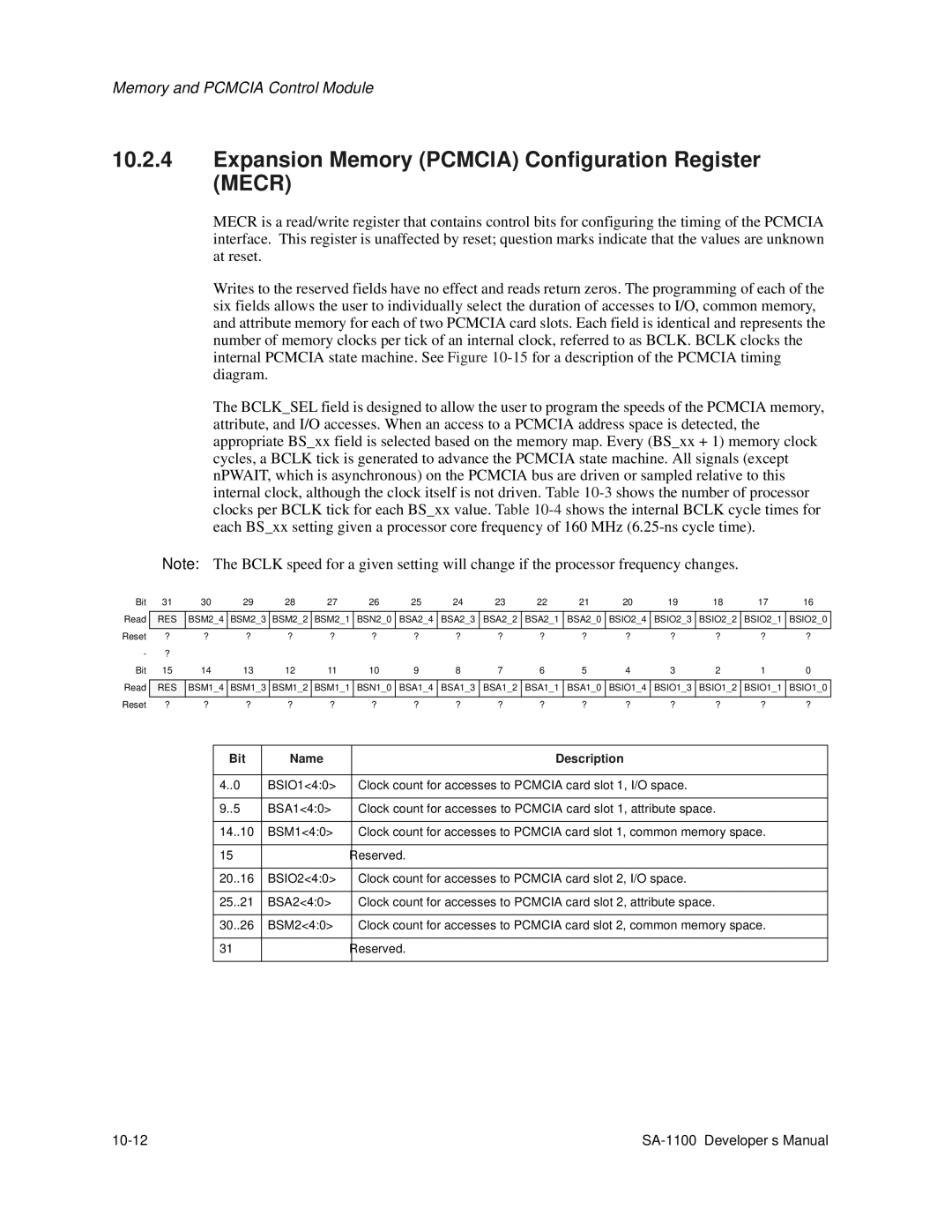
Expansion Memory Pcmcia Configuration Register Mecr
Bclksel
BSxx Bit Encoding
Bclk Speeds for 160-MHz Processor Core Frequency
Bclk Cycle Time-ns
Dram Memory Size Options
Dynamic Interface Operation
Dram Overview
Dram Row/Column Address Multiplexing
Dram Timing
Addr
Mdcnfgtrp = 4 MDCNFGCDB2 =
Dram Burst-of-Eight Transactions
Dram Refresh
Dram Self-Refresh in Sleep Mode
Static Memory Interface
10-18
ROM Timing Diagrams and Parameters
ROM Interface Overview
Input Data Latch
A255
A42
10-20
Eight Beat Burst Read from Burst-of-Four ROM
SA-1100 Developer’s Manual
Sram Timing Diagrams and Parameters
Sram Write Timing Diagram 4-Beat Burst
Sram Interface Overview
Flash Eprom Interface Overview
Flash Eprom Timing Diagrams and Parameters
10-24
Dram Access Followed by a Refresh Operation
Static Access Followed by a Dram Access
Dram Access Followed by a Static Access
General Memory BUS Timing
Pcmcia Overview
10-26
10.6.1 32-Bit Data Bus Operation
Address
External Logic for Pcmcia Implementation
10-28
12. Pcmcia External Logic for a Two-Socket Configuration
13. Pcmcia External Logic for a One-Socket Configuration
10-30
Pcmcia Interface Timing Diagrams and Parameters
14. Pcmcia Voltage-Control Logic
15. Pcmcia Memory or I/O 16-Bit Access
10-32
16. Pcmcia I/O 16-Bit Access to 8-Bit Device
Flow of Events After Reset or Exiting Sleep Mode
Initialization of the Memory Interface
10-34
Alternate Memory Bus Master Mode
Page
Peripheral Control Module
Read/Write Interface
Memory Organization
Peripheral Register Width DMA Burst Size
LCD Controller 0h B010 Serial Port
Peripheral Units’ Base Addresses
Peripheral Serial Protocol Base Address
ICP Hssp
Interrupt
Interrupts
Peripheral Units’ Interrupt Numbers
Peripheral
Peripheral Pins
Dedicated Peripheral Pins
Peripheral Gpio Pin Function
Use of the Gpio Pins for Alternate Functions
Peripheral Unit Gpio Pin Assignment
DMA Controller
DMA Register Definitions
DMA Device Address Register DDARn
D31 D0 1 0 from memory
Controller From Half-word wide
Device From To Half-word wide To From Byte-wide
Valid Settings for the DDARn Register
Ddar Fields Unit Name Function Address DA318 DS30
11-10
DMA Control/Status Register DCSRn
DMA Buffer a Start Address Register DBSAn
DMA Buffer a Transfer Count Register DBTAn
DMA Buffer B Transfer Count Register DBTBn
DMA Operation
DMA Buffer B Start Address Register DBSBn
TCB120 Transfer count buffer B
Physical Address Register Name Symbol
DMA Register List
DBSB3
DBSA3
DBTA3
DBTB3
LCD Controller
11-16
Lpclk
Frame Buffer
LCD Controller Operation
DMA to Memory Interface
11-18
PBS
To palette
13..12
Pixel bit size
Frame to palette
Encoded Pixel Data70 Bit
Unused Red Data30 Green Data30 Blue Data30
Encoded Pixel Data150
FrameBufferSize = 32 + 16 + è
11-22
Input Fifo
Lookup Palette
Color/Gray-Scale Intensities and Modulation Rates
Color/Gray-Scale Dithering
Output Fifo
Dither Value Intensity Modulation Rate
LCD Controller Pins
LCD Controller Register Definitions
Color/Monochrome Select CMS
LCD Enable LEN
LCD Controller Control Register
Single-/Dual-Panel Select SDS
Single Passive Screen Portion Pins
LCD Controller Data Pin Utilization
Dual Panel Active Panel
LCD Data-Pin Pixel Ordering
11-28
Error Interrupt Mask ERM
LCD Disable Done Interrupt Mask LDM
Base Address Update Interrupt Mask BAM
Passive/Active Display Select PAS
11-30
Double-Pixel Data DPD Pin Mode
Palette DMA Request Delay PDD
11.7.3.8 Big/Little Endian Select BLE
SDS
LEN
CMS
LDM
DPD
PAS
BLE
PDD
End-of-Line Pixel Clock Wait Count ELW
Pixels Per Line PPL
Horizontal Sync Pulse Width HSW
11-34
HSW
Beginning-of-Line Pixel Clock Wait Count BLW
PPL
ELW
Lines Per Panel LPP
Vertical Sync Pulse Width VSW
11-36
End-of-Frame Line Clock Wait Count EFW
Beginning-of-Frame Line Clock Wait Count BFW
EFW
LPP
VSW
BFW
Pixel Clock Divider PCD
AC Bias Pin Frequency ACB
Horizontal Sync Polarity HSP
AC Bias Pin Transitions Per Interrupt API
Vertical Sync Polarity VSP
Pixel Clock Polarity PCP
Output Enable Polarity OEP
Address 0h B010
PCP
LCD Controller DMA Registers
HSP
OEP
DBAR1
DMA Channel 1 Base Address Register
31..0
DMA channel 1 base address pointer
DMA channel 1 current address pointer
DMA Channel 1 Current Address Register
DCAR1
Equal to the calculated end address of the buffer
DCAR2
DMA Channel 2 Base and Current Address Registers
DBAR2
DMA channel 2 current address pointer
Bus Error Status BER read/write, maskable interrupt
LCD Disable Done Flag LDD read/write, maskable interrupt
Base Address Update Flag BAU read-only, maskable interrupt
LCD Controller Status Register
AC Bias Count Status ABC read/write, nonmaskable interrupt
LDD
BAU
IOL
BER
ABC
IUL
LCD Controller Register Locations
LCD Controller Control, DMA, and Status Register Locations
LCD Controller Pin Timing Diagrams
LDDx0
Lfclk Llclk Lpclk
LDDx0
11-52
12. Passive Mode Pixel Clock and Data Pin Timing
DPD =
13. Active Mode Timing
11-54
14. Active Mode Pixel Clock and Data Pin Timing
Serial Port 0 USB Device Controller
USB Operation
11-56
Bus State UDC+/UDC- Pin Levels
Signalling Levels
10. USB Bus States
Port
Bit Encoding
Bit Value Digital Data Nrzi Data
11-58
Endpoint Field Value UDC Endpoint Selected
Field Formats
11. Endpoint Field Addressing
Endpoint
CRC5
Packet Formats
PID
CRC16
OUT
Transaction Formats
Action
Packets from UDC to host are boldface
Action Token Packet Data Packet
Setup DATA0
UDC Device Requests
11-62
UDC Register Definitions
12. Host Device Request Summary
Request Name
UDC Control Register
Address 0h 8000
Reset Interrupt Mask REM
Suspend/Resume Interrupt Mask SRM
Udccr
Udcar
UDC Address Register
UDC OUT Max Packet Register
Udcomp
UDC in Max Packet Register
Address 0h 8000 000C
Udcimp
UDC Endpoint 0 Control/Status Register
SSE FST SST IPR OPR
Serviced Setup End SSE
UDCCS0
SSE
UDC Endpoint 1 Control/Status Register
Receive Fifo Service RFS
Receive Packet Error RPE
Receive Packet Complete RPC
RNE FST SST RPE RPC RFS
Bits 7..6 Reserved
UDCCS1
RNE
UDC Endpoint 2 Control/Status Register
Transmit Fifo Service TFS
Transmit Packet Error TPE
Transmit Packet Complete TPC
UDCCS2
FST SST TUR TPE TPC TFS
UDCD0
UDC Endpoint 0 Data Register
UDC Endpoint 0 Write Count Register
Data
Top/bottom of transmit/receive Fifo data
UDC Data Register
Uddr
Read Bottom of receive Fifo data
UDC Status/Interrupt Register
Rstir Resir Susir TIR RIR EIR
Reset Interrupt Request Rstir
Udcsr
Rstir
Serial Port 1 SDLC/UART
UDC Register Locations
13. UDC Control, Data, and Status Register Locations
Sdlc Operation
Control Field
Frame Format
Address Field
CRC-CCITT
Data Field
CRC Field
Baud Rate Generation
Receive Operation
11-82
Transmit Operation
Simultaneous Use of the Uart and Sdlc
Transmit and Receive FIFOs
CPU and DMA Register Access Sizes
Sdlc Register Definitions
11-84
SDLC/UART Select SUS
Loopback Mode LBM
Sdlc Control Register
Single/Double Flag Select SDF
Sample Clock Direction SCD
Sample Clock Enable SCE
Bit Modulation Select BMS
11-86
Address 0h 8002
Receive Clock Edge Select RCE
Transmit Clock Edge Select TCE
SDCR0
Abort After Frame AAF
TCE
Receive Fifo Interrupt Enable RIE
Transmit Enable TXE
Receive Enable RXE
Transmit Fifo Interrupt Enable TIE
Transmit Fifo Underrun Select TUS
Address Match Enable AME
Receiver Abort Interrupt EnableRAE
11-90
RAE TUS AME TIE RIE RXE TXE AAF
SDCR1
Read/Write
RAE
Address Match Value AMV
SDCR2
AMV
Address 0h 8002 006C
Sdlc Control Registers 3
Baud Rate Divisor BRD
SDCR3
Sdlc Data Register
11-94
ROR CRE EOF
Address 0h 0078
Sddr
ROR
Receiver Abort Status RAB read/write, maskable interrupt
Sdlc Status Register
Transmit Underrun Status TUR read/write, maskable interrupt
11-96
SA-1100 Developer’s Manual 11-97
SDSR0
RFS TFS RAB TUR EIF
Receive Fifo Not Empty Flag RNE read-only, noninterruptible
Receiver Synchronized Flag RSY read-only, noninterruptible
Transmitter Busy Flag TBY read-only, noninterruptible
Transmit Fifo Not Full Flag TNF read-only, noninterruptible
CRC Error Status CRE read-only, noninterruptible
Receiver Overrun Status ROR read-only, noninterruptible
11-100
RSY
SDSR1
ROR CRE EOF RTD TNF RNE
TBY
Uart Register Locations
14. Uart Control, Data, and Status Register Locations
Serial Port 2 Infrared Communications Port ICP
Sdlc Register Locations
15. Sdlc Control, Data, and Status Register Locations
Uart Frame Format
Low-Speed ICP Operation
HP-SIR*Modulation
11-104
High-Speed ICP Operation
11.10.2.1 4PPM Modulation
Chip Timeslots Data =
Hssp Frame Format
SA-1100 Developer’s Manual 11-107
11-108
SA-1100 Developer’s Manual 11-109
11-110
Uart Register Definition
HP-SIR Enable HSE
Low-Power Mode LPM
Uart Control Register
IrDA Transmission Rate ITR
Hssp Register Definitions
Hssp Control Register
LPM
SA-1100 Developer’s Manual 11-113
11-114
Address 0h 8004
HSCR0
AME TIM RIM RXE TXE TUS LBM ITR
HSCR1
Search for the next preamble
11-116
Transmit Pin Polarity Select TXP
Receive Pin Polarity Select RXP
RXP TXP
0h 9006
HSCR2
RXP
Hssp Data Register
Last Fifo entry is transferred to the ROR bit
Address 0h 8004 006C
Hsdr
HSSR1
Hssp Status Register
Receiver Abort Status RAB read/write, nonmaskable interrupt
11-122
FRE RFS TFS RAB TUR EIF
Framing Error Status FRE read/write, nonmaskable interrupt
HSSR0
FRE
End-of-Frame Flag EOF read-only, noninterruptible
11-124
SA-1100 Developer’s Manual 11-125
HSSR1
ROR CRE EOF TNF RNE TBY RSY
Hssp Register Locations
16. Uart Control, Data, and Status Register Locations
17. Hssp Control, Data, and Status Register Locations
LSB MSB
Serial Port 3 Uart
Uart Operation
11-128
30. NRZ Bit Encoding Example 0100
11-130
Parity Enable PE
Uart Register Definitions
11.11.3.2 Odd/Even Parity Select OES
Stop Bit Select SBS
Data Size Select DSS
11-132
UTCR0
TCE RCE SCE DSS SBS OES
UTCR1
Bit Reset BRD70
Uart Control Registers 1
UTCR2
Receiver Enable RXE
Transmitter Enable TXE
Break BRK
UTCR3
LBM TIE RIE BRK TXE RXE
Uart Data Register
Utdr
ROR FRE PRE
Uart Status Register
Error in Fifo Flag EIF read-only, nonmaskable interrupt
Receiver Idle Status RID read/write, maskable interrupt
11-140
Address 0h 8005 001C
UTSR0
EIF REB RBB RID RFS TFS
Parity Error Flag PRE read-only, noninterruptible
11-142
Framing Error Flag FRE read-only, noninterruptible
Receiver Overrun Flag ROR read-only, noninterruptible
UTSR1
Read-Only
ROR FRE PRE TNF RNE TBY
Serial Port 4 MCP / SSP
MCP Operation
11-146
31. MCP Frame Data Format
Audio and Telecom Sample Rates and Data Transfer
11-148
MCP Transmit and Receive Fifo Operation
Codec Control Register Data Transfer
Bit Audio Data Telecom Data
11-150
External Clock Operation
Alternate SSP Pin Assignment
Audio Sample Rate Divisor ASD
MCP Register Definitions
MCP Control Register
11-152
Telecom Sample Rate Divisor TSD
External Clock Select ECS
Multimedia Communications Port Enable MCE
11.12.3.5 A/D Sampling Mode ADM
11-154
Audio Transmit Fifo Interrupt Enable ATE
Telecom Transmit Fifo Interrupt Enable TTE
Telecom Receive Fifo Interrupt Enable TRE
Audio Receive Fifo Interrupt Enable are
Audio sample rate divisor
External Clock Prescaler ECP
ASD
TSD
ADM
MCE
ECS
TTE
MCP Data Registers
Clock Frequency Select CFS
CFS
Reserved for future enhancements
MCP Data Register
Address 0h 8006 MCP Data Register 0 MCDR0 Read/Write
15..4
Address 0h 8006 000C MCP Data Register 1 MCDR1 Read/Write
SA-1100 Developer’s Manual 11-161
15..0 Codec
Reg Address R/W Reset Bit
Address 0h 8006 MCP Data Register 2 MCDR2 Read/Write
Register read Read/write Read Returns a zero
MCP Status Register
11-164
SA-1100 Developer’s Manual 11-165
Codec Write Completed Flag CWC read-only, noninterruptible
Audio Codec Enabled Flag ACE read-only, noninterruptible
Telecom Codec Enabled Flag TCE read-only, noninterruptible
Codec Read Completed Flag CRC read-only, noninterruptible
TTS
ATS
ARS
TRS
ANF
TTU
TRO
ANE
SSP Operation
35. Texas Instruments* Synchronous Serial Frame Format
11-170
36. Motorola* SPI Frame Format
37. National Microwire* Frame Format
11-172
SSP Transmit and Receive FIFOs
Bit Bit Data
SSP Register Definitions
SSP Control Register
11-174
Synchronous Serial Port Enable SSE
Frame Format FRF
Serial Clock Rate SCR
FRF
SCR
Serial Clock Polarity SPO
LSB
Serial Clock Phase SPH
Sclk SPO=0 Sclk SPO=1 Sfrm TXD4 RXD4
11-178
SPO
SSP Data Register
Address 0h 8007 006C
Justifies data and zero fills unused bits 11-180
SSP Status Register
SSP Busy Flag BSY read-only, noninterruptible
BSY
19. MCP Control, Data, and Status Register Locations
MCP Register Locations
SSP Register Locations
20. SSP Control, Data, and Status Register Locations
Peripheral Pin Controller PPC
PPC Operation
11-184
PPC Register Definitions
PPC Pin Direction Register
Sclk
PPC Pin State Register
Address 0h 9006 Ppsr PPC Pin StateRegister Read/Write
LCD line clock pin state
LCD pixel clock pin state
Read Current state of LCD pixel clock pin returned
Read Current state of LCD line clock pin returned
SSP Pin Reassignment SPR
PPC Pin Assignment Register
Uart Pin Reassignment UPR
UPR
PPC Sleep Mode Pin Direction Register
11-190
LCD line clock sleep mode pin direction
LCD pixel clock sleep mode pin direction
LCD pixel clock pin configured as input during sleep
LCD line clock pin configured as input during sleep
PPC Pin Flag Register
PPC Register Locations
21. PPC Control and Flag Register Locations
Page
Absolute Maximum Ratings
Symbol Parameter Min Max Units
DC Parameters
SA-1100 DC Maximum Ratings
SA-1100 DC Operating Conditions
Symbol Parameter Min Nom Max Units
DC Operating Conditions
× Vddx
VDD
Power Supply Voltages and Currents
Parameter SA-1100 Units
Vddx
Page
AC Parameters
Test Conditions
SA-1100 Output Derating
Memory Bus Memory Bus Out
Memory Bus and Pcmcia Signal Timings
Module Considerations
13-2
LCD Controller Signals
MCP Signals
LLDD70 fall
SA-1100 AC Timing Table for AA and BA Parts
Pin Name Symbol Parameter Min Max Unit
Timing Parameters
Sfrmc
Asynchronous Signal Timing Descriptions
Page
Package and Pinout
Mechanical Data and Packaging Information
SA-1100 Pinout 208-Pin Quad Flat Pack
14-2
Mini-Ball Grid Array mBGA
SA-1100 256 Mini-Ball Grid Array Mechanical Drawing
SA-1100 Pinout 256-Pin Mini-Ball Grid Array
14-4
Debug Support
Instruction Breakpoint
Data Breakpoint
Page
Test Access Port TAP Controller State Transitions
Boundary-Scan Test Interface
Instruction Register
Reset
Pull-Up Resistors
Public Instructions
Extest
SAMPLE/PRELOAD
Clamp
Bypass
Highz
Idcode
16-4
Test Data Registers
Bypass Register
16.6.2 SA-1100 Device Identification ID Code Register
16.6.3 SA-1100 Boundary-Scan BS Register
16-6
Tbsis Tbsih
Boundary-Scan Interface Signals
Tbscl Tbsch
Tbsoh Tbsod Data Tbsss Tbssh Data Out Tbsdh Tbsdd
Tbsr
Tbsoe
Data Out Tbsde
Tbsrs Tbsrh
Symbol Parameter Minimum Typical Maximum Units
SA-1100 Boundary-Scan Interface Timing
Page
Register Summary
Tucr
B000 0048 Write ones to clear 004C Read only 0050
B000 0044
DMA control/status register 2 write ones to set
B000 0054
Ucdomp
8003 Reserved 8003 001C
Sdlc Registers Serial Port 8002
8031
8004 007C 0h 8004 Ffff Reserved
Uart Registers Serial Port 8005
8007 0078 0h 8007 Ffff Reserved PPC Registers 9006
9006 0034 0h 9006 Ffff Reserved
MHz Oscillator Specifications B
Specifications
System Specifications
MHz Oscillator Specifications
Specification Minimum Typical Maximum Unit
Quartz Crystal Specification
Specification
Typical Maximum Unit
Page
Current Consumption
KHz Oscillator Specifications C
Temperature Range
Startup Time
Parasitic Resistance Between Txtal and Textal
Frequency Shift Due to Temperature Effect on the Circuit
Parasitic Capacitance Off-chip Between Txtal and Textal
Parasitic Resistance Between Txtal or Textal and VSS
Corresponding to specified range of Rm are supplied
Other providers supply a Quality Factor, Q, instead of Rm
Therefore, the values for Q
Following table
KHz Oscillator Specifications
Internal Test
Test Unit Control Register Tucr
PMD
TSEL2-0
TSEL2 TSEL1 TSEL0
Page
Support, Products, and Documentation