ERserver
Page
ERserver
Sixth Edition August
Contents
Service Reference
Initial Program Load IPL Information
Trademarks
Appendix A. OS/400 Operating System
Vii
Safety and Environmental Notices
Environmental Design
Battery Return Program
Product Recycling and Disposal
Safety and Environmental Notices
Service Functions V5R2
Prerequisite and related information
About Service Functions SY44-5902-03
Who should read this book
Conventions and terminology used in this book
ISeries Navigator
How to send your comments
Introduction
Dedicated Service Tools DST
Dedicated Service Tools requirements
Limited paging
System paging environments
Stand-alone paging non-paging
Full paging
Performing an IPL to DST
Accessing Dedicated Service Tools
This ends the procedure
Changing a service tools user ID
Performing an IPL to DST for secondary partitions
Resetting Qsecofr service tools user ID
Selecting Function 21 while the system Is operational
Performing an alternate IPL to DST type D IPL
Function keys in DST
Paging environment DST options IPL non-paging Limited Full
Exiting Dedicated Service Tools
DST options
Work with Licensed Internal Code
Installing Licensed Internal Code
Installing the operating system
Perform an IPL
Options and function keys
Licensed Internal Code general information
Work with disk units
Paging environment Work with disk unit options
Options on the Work with Disk Units Display
Paging environment Work with disk unit options
Paging environment Work with disk unit options
Work with ASPs threshold
Display disk configuration
Add units to ASPs
Add units to ASPs and balance data
Display disk configuration status
Enable remote load-source mirroring
Disable remote load-source mirroring
Start compression on non-configured disk units
Change ASP storage threshold
Remove units from configuration
Delete user ASP
Delete ASP data
Exclude unit in device parity protection
Restore disk unit data
Start device parity protection
Stop device parity protection
Replace disk unit
Recover disk configuration
Disk unit problem recovery procedures
Upgrade load-source utility
Reclaim IOP cache storage
Recover unknown load source
Recover mirrored load source
Recover from start compression failure
Work with Dedicated Service Tools environment
Work with active service tools
Selecting Console Type
Work with service tools user IDs
Work with system devices
Resource Name
Device ID
Work with system values
Options on the DST Console Mode display
Work with alternate installation device
Select DST console mode
Options on the Start a Service Tool display
Start a service tool
Dump to media
Main storage dump manager option allows you to
Dedicated Service Tools DST
Service Functions V5R2
Status Conditions
Options and Function Keys
Starting
Condition Description Waiting
Stopping
Stopped
Start Trace
Format and print trace
Select the Work with communications traces option
Example Format Trace Data Display
Record status
Record timer
Record number
Data length
Controller name/number
Perform automatic installation of the operating system
Save Licensed Internal Code
Work with save storage and restore storage
Work with remote service support
Work with remote service support option allows you to
Activating remote service support
Allowing access for remote service support
Work with system security
Work with system partitions
Work with system capacity
Dedicated Service Tools DST
Service Functions V5R2
Hardware Service Manager
Hardware Service Manager options
Packaging hardware resources
Paging environment Hardware service manager options
Example Packaging Hardware Resources display
Logical hardware resources
Example Logical Hardware Resources display
Locate resource by name
Example Locate Resource By Resource Name display
Example Logical Hardware Resource display
Failed and non-reporting resources
No failed logical hardware resources were found
Battery power unit information
System Power Control Network Spcn
Example Service Action Log Report display
Work with service action log
SRC field
Option field
Status field
Date and time fields
Display label location work sheet
Device concurrent maintenance
Frame serial number
Frame ID
Position
Device resource name
Action to be performed
Time delay needed in minutes
From packaging displays
Change resource details
Example Change Packaging Hardware Resource Detail display
From logical displays
Example Change Logical Hardware Resource Detail display
Concurrent maintenance
DB1
Create frame information
Example Select Packaging Model display
Debug the resource
Display associated resources
Display address
Communications IOA 2620-001
Display card gap information
From Hardware Service Manager display
Display hardware contained within package
Display failed resources
Display non-reporting resources
Display location information
Display resources associated with IOP
CMB01
Display resource details
Actual type-model
Resource name
Description
Type-model
Location text
Alternate service node
Alternate service telephone
Service provider
Shared by multiple systems
Manufactured by IBM
Example Hardware Resources That Require Attention display
Display resources requiring attention
Example Hardware Resource Attention Message display
Display resource status
From the Logical Hardware Resources display
Display system bus resources
Service Functions V5R2
Example Logical Hardware Resources on System Bus display
Display unresolved locations
Display system information
From packaging and logical displays
Print
Refresh the display
Remove non-reporting resource information
Reserve frame space
Using High-Speed Link HSL specific options
BCC02
Display detail
This display shows the details of an HSL I/O bridge resource
Not operational
Type-model
Unknown
Operational
Enabling
Enabled
Disabled
Not Available
Link Speed
Display system information
Internal
External
Example Port Connection Information display
Display port information
Example Logical Hardware Associated With HSL Loops display
Resources associated with loop
SPD02
Verify resources
Symbol Description
Symbols on the Hardware Service Manager displays
Printing the System Configuration List
This ends the procedure
Hardware Service Manager Verify
Verification procedures
Verify tape
Verify optical storage unit
Verify diskette
Communications test descriptions
Verify communications
Service Functions V5R2
Product Activity Log
Use the Product Activity Log option to
Service Action Log SAL
Product Activity Log PAL
Paging environment
Recovering from Product Activity Log errors while in DST
Product Activity Log location
Analyze log
Options and function keys
Example Select Analysis Report Options display
Display or print by log ID
Work with removable media lifetime statistics
Change Product Activity Log sizes
Sort by ... function
Symbol Explanation Action
Display or print removable media session statistics
Example Log Summary by Resource Name
Address information function
Hexadecimal Product Activity Log data
View description function
Example Hexadecimal Detail Report for Resource
Example Hexadecimal Report for Resource
Interpreting Product Activity Log reports
Resource Type Model Serial number Volume ID
Subsystem Possible Names
Resource name
Data protection lost
Resource type, model, and location
Class
System reference code
Unit Address Value Unit Address Data Definition
Multiple SRC entries
Logical address format
IPL source/state
Sequence number
Secondary code
Table ID
Srid
Hexadecimal offset Length in bytes Description
More information from hexadecimal reports
Device Formatting Log Example unformatted information
Example Hexadecimal Report, Device Formatting Log Template
Array Member Formatting Log Example unformatted information
Configuration Formatting Log Example unformatted information
Configuration Formatting Log Template
Needvalidp N
Array Addendum Log Template
Setting the system date and time
Service Reference Procedures
Determining the dominant operating system
System password
System unique identifier
Primary console requirements
Identifying the consoles when the system is operational
Determining a primary or alternative console Introduction
Select the Associated packaging resources option
Locating the system’s load source from the system console
History file
Getting started
Continuously Powered Main Storage CPM
Low-level debug and data collecting procedures Introduction
Function Description Range
Following table
Introduction
Changing the address
For PowerPC-based IOPs Setting the ww Position
Setting the yy Position
Setting the zz Position
Setting the xx Position
Setting the ww Position
Logical partitions
Displaying data from function
137
Select Display partition information
Determining the release level of a logical partition
Locating a secondary partition’s console
Yes No
Select Hardware Service Manager
Yes No ↓ This ends the procedure
Locating a secondary partition’s load source
Yes No
Finding the SRC history list for a secondary partition
Closing related problems in other logical partitions
Querying logical partition time and date
Press the function key for Include Reference Code Detail
Accessing the panel functions of a logical partition
Select Work with Partition Status
Select the Work with system partitions options. option
Selecting IPL source and mode for a secondary partition
Options on the Work with Partition Status display
Example of Work with Partitions Status display
= Power on
11 = Mode auto
= Delayed power off
= Mode normal
10 = Mode manual
Guest partitions
Determining the hosting partition of a guest partition
Determining if the system has guest partitions
Determining the release level of a guest partition
Service Reference Procedures
Determining the power controlling system of a tower
Example Display HSL System Information display
Service Functions V5R2
This ends the procedure
Switching ownership of a tower’s switchable resources
Example I/O Debug Function display
Example Confirm Ownership Change display
Switching the mode of a tower’s switchable resources
Example Confirm Mode Change display
This ends the procedure
Values for IPL types, key modes, and speeds
Control Panel Functions
Function code Function selected
Disable CPM
System status SRC trace
Displays are F, S, SE, V=F, or V=S
Function/data Action or description
Mode combinations AN, BN, CN, DN, AM, BM, CM, DM
Function/data Action or description
Function / value Action or description
Spcn SRC Formats
Function / data Action or description
Cancel Request
System Power On
Bulk Power On
Fan Power Off
Bulk Power Off
Fan Power On
Tmmm cccc
Service Functions V5R2
Function Subfunction Data Display
Service Functions V5R2
Control Panel Functions
Control panel functions Models 270, 8xx, SB2, SB3,
Ways to access the control panel Models 270, 8xx, SB2, SB3,
ISeries control panel without a keystick
Customer control panel functions Models 270, 8xx, SB2, SB3,
Function 01 on systems with a keystick
Press Enter to select the IPL type and exit
Current IPL type is displayed with a
N S
Function Action or description
Support-directed procedure only
Fans Power supplies
Operations diagram for functions A6 and A8
This ends the procedure
Customer Extended Panel Functions Models 270, 8xx, SB2, SB3
Extended control panel functions Models 270, 8xx, SB2, SB3
Service Extended Panel Functions Models 270, 8xx, SB2, SB3
5700
Select Function 53 and press Enter to display
Control Panel Functions
Service Functions V5R2
SRC formats
System Reference Code SRC Information
Example SRC record structure all models
Models 270, 8xx, SB2, and SB3
Function display Description
Problem
Word 1 SRC general information
Identifying SRCs
Word 2 System status information
Status indicators
Hex Digit IPL State Description
IPL Type a IPL Type B IPL Type C IPL Type D
System Reference Codes SRCs
General system and Unit Reference Code URC information
System Reference Codes SRCs
Lmmm
Lmmm
Rrrr LIC unit reference code URC
Tttt Outboard failing unit type number for example
Pxxx
Mmmm
LIC Unit Reference Code Groups
Bbbb Ccbb
4A-4F
20-27
440x
441x
IPL status SRCs
Spcn informational concurrent maintenance SRCs
C1xx B1xx
C1xx 100C
C100
C200 12FF
C100 D009
C200
C200 11FF
C200 51FF
C200 43FF
C3xx
C200 71FF
C200 81FF
C200 82FF
LIC is initializing the Load Source IOP messaging functions
Initialize RM component process management
Authority recovery is running
C600 432B
C600 432A
C600 450A
End of CPM IPL SRCs
C600 4B57
C600 450C
C600 4A57
C600 4A60
C900 2A80
C900 29A0
C900 29B0
C900 29C0
C900 2AA1
C900 2A90
C900 2A95
C900 2AA0
General status SRCs
D900 27C0
D6xx
D900
Service Functions V5R2
Methods to perform IPL
Initial Program Load IPL Information
IPL type, mode, and speed options
IPL speed recommendations
IPL sequence
Alternate installation IPL
Service processor initialization
What is initialized
Abnormal ending
Licensed Internal Code LIC initialization
Log entries
Initialization output
Data descriptions
Status SRCs
Service Functions V5R2
Fixes and cumulative PTF packages
Licensed Internal Code
Licensed Internal Code LIC introduction
Displaying Licensed Internal Code fixes
Cumulative PTF packages
PSP listings
Licensed programs
Group Name Description
Overview of Licensed Internal Code Install and Restore
Code naming conventions
Installing Licensed Internal Code
Utility to install Licensed Internal Code
Restoring Licensed Internal Code
Utility to restore Licensed Internal Code
Authorized Program Analysis Report Apar
229
System Architecture and Configuration
Hardware information
System power overview Power supply
Battery power unit
Secondary node
Spcn power components
Primary node
Spcn addressing
Spcn menu flow
System Architecture and Configuration
Unit
Battery capacity test
Opt
Frame
Write Vital Product Data VPD option
Fault
Display Detail option
Cable type for connector J16
Power sequence complete
Uepo switch
Cable type for connector J15
Battery present
Next battery capacity test time
Last battery capacity test date
Last battery capacity test time
Next battery capacity test date
Test battery option
High Speed Link
System Interconnect
Resource names
Multi-adapter bridge
Name Description Example
Manager on page 45 and , Product Activity Log on
Hardware configuration restrictions
Wrap connector pin to pin Connector pin Signal destination
High speed communications card and wrap connector wiring
Advanced PCI communications console cable
Cryptographic processor card and wrap connector wiring
Signal designation
Wrap connector pin to pin
Two-port 232/ac dc
Wrap connector pin to pin Connector pin
Isdn wrap connector and connector pin
Two-port communications adapter cable
Two-port communications adapter cable wiring
Description Pin
RJ-45 cable wrap connector
Communications adapter remote power-on cable
Wrap connector pin to
24/X.21bis communications adapter cable
EIA 232 advanced PCI communications cable
Stage 1 V.24/X.21bis cable wrap connector wiring
24/X.21bis cable wrap connector wiring
Signal designation Wrap connector pin to pin
Stage 1 EIA-232/X.21bis communications adapter cable
EIA 232 advanced wrap connector wiring
Signal destination Wrap connector pin to pin
EIA-232/X.21bis communications adapter cable
EIA-232/X.21bis cable wrap connector wiring
Rlsd A, B
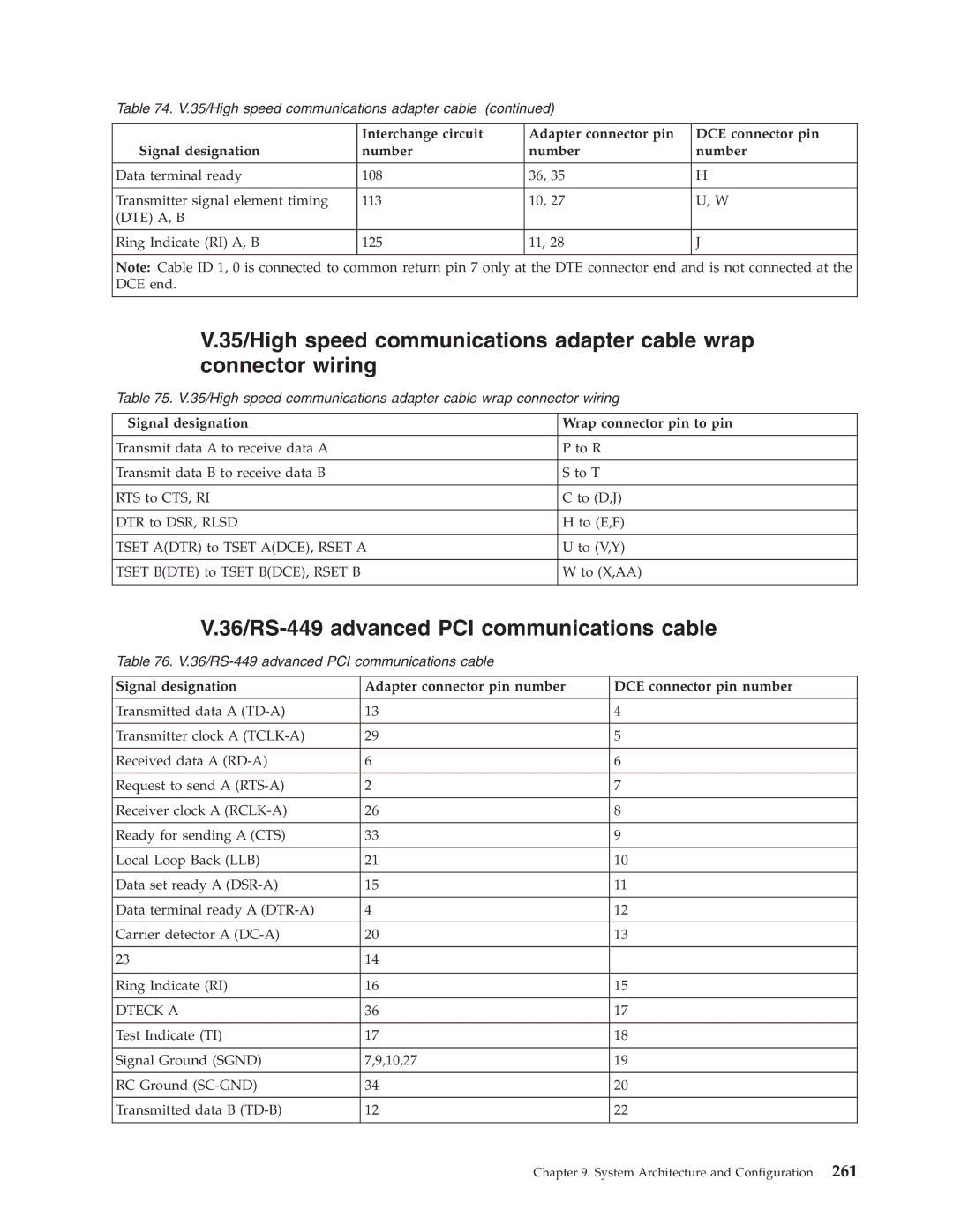
36/EIA 449 high speed communications adapter cable
Advanced PCI communications cable
Stage 1 V.35 cable wrap connector wiring
Stage 1 V.35 communications adapter cable
Advanced wrap connector wiring
35 advanced wrap connector wiring
35/High speed communications adapter cable
Cable wrap connector wiring
Communications adapter cable
36/RS-449 advanced PCI communications cable
DTR-A DSR-A, CD-A
36/RS-449 advanced cable wrap connector wiring
21/High speed communications adapter cable
Ethernet/IEEE 802.3 transceiver adapter cable and card wrap
Token-ring communications adapter cable and card wrap
DDI transceiver adapter cable and card wrap
Facsimile adapter cable wrap connector wiring
Signal designation Wrap connector port a pin to port B pin
Unused
PCI communications card wrap connector wiring
Interface type OFF voltage level On voltage level
Communications signal voltage levels
Service Functions V5R2
Main storage dump introduction
Working with Storage Dumps
Automatic main storage dump
Performing a main storage dump to disk manual MSD
Copying a main storage dump
Work with current main storage dump
Copy main storage dump to MSD copy
Work with copies of main storage dumps
Display main storage dump
Copy main storage dump to media
MSD status Function performed
Main storage dump status
Terminating System Reference Code SRC
MSD status
Reporting the error
Additional help
Copying the IOP storage dump to removable media All Models
IOP dump information in the Product Activity Log All Models
Service Functions V5R2
DST in OS/400 full paging environment
Appendix A. OS/400 Operating System
DST in OS/400 limited paging environment
System Service Tools SST
Accessing system service tools
SST options
Selecting SST from the problem handling option
Entering the Start System Service Tools Strsst command
Start a service tool
Options
Work with diskette data recovery
Work with disk units
Appendix A. OS/400
Example of Alter Diskette Data display
Example of Display Diskette Data display
How to use the Work with Diskette Data Recovery option
Work with system security
Function keys SST
Work with system partitions
Work with system capacity
System-detected problems
Online problem analysis and resolution Introduction
Messages relating to hardware failures
Problem log
Customer-detected problems
OS/400 or LIC Apar information
Service support facility
Displaying OS/400 PTFs
Task to be performed What to do Location of instructions
ISeries Information Center, Problem
Varying configuration descriptions on and off
OS/400 Command Function
Commonly used OS/400 service commands
Endrmtspt
Wrkhdwprd
Work with System Value Wrksysval Command
Commonly used system values
Service attributes Dspsrva or Chgsrva commands
Commonly used service attributes
Chgsrva CRITMSGUSR*QSYSOPR
Change Transmit Level Chgxmtlvl command
Work with Hardware Products Wrkhdwprd Command
Work with Hardware Products display appears
Save the system configuration data to the file you created
Change Description Label Locations display appears
Location
Change Description Label display appears
Commonly used verify commands
Verify commands
Test descriptions
Procedure
Service Functions V5R2
Appendix A. OS/400
External ring test
Appendix A. OS/400
Service Functions V5R2
Appendix A. OS/400
Status Data Action
Communications tests Wireless LAN adapter card indicators
Communications interface trace
Test description
Concurrent LPDA-2 tests
Service Functions V5R2
Appendix A. OS/400
Service Functions V5R2
321
Appendix B. Notices
IBM
Trademarks
Appendix B. Notices
Service Functions V5R2
BAT. See basic assurance test
Glossary of Terms and Abbreviations
Cpi. See characters per inch
EBCDIC. See extended binary-coded decimal interchange code
IPL. See initial program load
SCS. See SNA character string
Type D IPL. See installation IPL
AER
Index
Vfycmn
Debug
Normal
335
LIC SRCs
See Misr
PAR
339
See also URCs for
Please tell us how we can improve this book
Readers’ Comments We’d Like to Hear from You
How satisfied are you that the information in this book is
Business Reply Mail
Page
SY44-5902-05