DS33R11
Part Temp Range PIN-PACKAGE
Table of Contents
Integrated T1/E1/J1 Transceiver
Device Registers
Operating Parameters
List of Figures
308
List of Tables
Description
Page
Microprocessor Interface
X.86 Link Access Protocol for SONET/SDH Ethernet Mapping
General
Hdlc Ethernet Mapping
Committed Information Rate CIR Controller
Sdram Interface
MAC Interface
T1/E1/J1 Line Interface
Clock Synthesizer
Jitter Attenuator
12 T1/E1/J1 Framer
TDM Bus
Test and Diagnostics
Specifications Compliance
T1-Related Telecommunications Specifications
Ethernet-to-WAN Extension With or Without Framing
CRC
B8ZS
BOC
ESF
Major Operating Modes
Rtip Rring MUX
Clad Ttip Transmit Framer MUX Tring
Bert
JTAG2 Transmit Serial Port Packet HDLC/X.86 CIR Controller
Clock
Jtag Host Interface
Receive and Transmit T1/E1/J1 LIU
Data
Loopback Sync Framer
Rlink
Sync Rsync Rmsync Rfsync Internal Rdata Signals Rchclk From
Sync Signaling Tseri Tsig
Rlclk
Pin Functional Description Detailed Pin Descriptions
Name PIN Type Function Microprocessor Port
IOZ
Read Data Strobe Intel Mode The DS33R11 drives the data bus
Name PIN Type Function
Chip Select for Protocol Conversion Device This pin must be
Name PIN Type Function MII/RMII PHY Port
Receive Data 0 through 3 MII Four bits of received data
Receive Data 0 through 1 Rmii Two bits of received data
Transmit Data 0 through 1RMII Two bits of data TXD
Reference Clock Rmii and MII When in Rmii mode, all signals
Transmit Data 0 through 3MII TXD 30 is presented
Reference Clock Output Rmii and MII a derived clock output
Name PIN Type Function PHY Management BUS
Sdram Interface
Sdcs
Sdram Data Bus Bits 0 to 31 The 32 pins of the Sdram data
Name PIN Type Function T1/E1/J1 Analog Line Interface
T1/E1/J1 Transmit Framer Interface
Ethernet Mapper Transmit Serial Interface
T1/E1/J1 Receive Framer Interface
Receive System Clock for the Transceiver 1.544MHz
Receive Frame Sync Pre Receive Elastic Store for T1/E1/J1
Receive Multiframe Sync for the T1/E1/J1 Transceiver An
T1/E1/J1 FRAMER/LIU Interim Signals
Transmit Elastic Store Output Updated on the rising edge
Transmit Negative-Data Output Updated on the rising edge
Transmit Positive-Data Output Updated on the rising edge
Transmit Clock Output from the T1/E1/J1 Framer Buffered
T1/E1/J1 Receive Signaling-Freeze Output Set high when
Name PIN Type Function Hardware and Status Pins
Mode Control for Processor Interface
Queue Overflow for Ethernet Mapper This pin goes high when
Name PIN Type Function System Clocks
Name PIN Type Function Jtag Interface
Receive Analog Signal Ground Connect to the common supply
Name PIN Type Function Power Supplies
Receive Analog Positive Supply Connect to 3.3V power supply
Transmit Analog Signal Ground Connect to the common supply
Ball BGA Pinout
Functional Description
Clear on Read
Processor Interface
Read-Write/Data Strobe Modes
Interrupt and Pin Modes
Rmiimiis Speed DCE/ DTE Refclko Rxclk PIN Output Input
Ethernet Mapper Clocks
Clocking Options for the Ethernet Interface
Txclk
T1/E1/J1
Ethernet MAC
Bert Refclk Arbiter
Ethernet Interface Clock Modes
Serial Interface Clock Modes
Resets and Low Power Modes
Reset Functions
Reset Function Location Comments
Per-Port Resources
Initialization and Configuration
Global Resources
Example Device Initialization Sequence
Device Interrupts
Drawing Legend
Pin
Information Registers
Interrupt Information Registers
Status Registers
Serial Interface
Connections and Queues
Registers Related to Connections and Queues
Arbiter
Register Function
Type Mode
Flow Control
Options for Flow Control
Full Duplex Flow Control
Half Duplex Flow Control
Host-Managed Flow Control
Ethernet Interface Port
Ieee 802.3 Ethernet Frame
Registers Related to Setting the Ethernet Port
Register Name Function
Configured as DTE Connected to an Ethernet PHY in MII Mode
DTE and DCE Mode
DS33R11 Configured as a DCE in MII Mode
Ethernet MAC
MAC Control Registers
MAC Status Registers
Address Register Description
MII Mode Options
Rmii Mode
Bert Features
Bert in the Ethernet Mapper
PHY MII Management Block and Mdio Interface
Receive Data Interface
Receive Pattern Detection
Prbs Synchronization
Repetitive Pattern Synchronization
Pattern Monitoring
Pattern Generation
Error Insertion
Performance Monitoring Update
Transmit Packet Processor
Receive Packet Processor
11. Hdlc Encapsulation of MAC Frame
19 X.86 Encoding and Decoding
12. Laps Encoding of MAC Frames Concept
13. X.86 Encapsulation of the MAC frame
Page
Committed Information Rate Controller
10.1 T1/E1/J1 Clocks
T1/E1/J1 Clock Map
10.3 T1/E1/J1 Transceiver Interrupts
T1/E1/J1 Transmit Clock Source
Per-Channel Operation
TCSS1 TCSS0 Transmit Clock Source
10.4 T1 Framer/Formatter Control and Status
10.4.1 T1 Transmit Transparency
AIS-CI and RAI-CI Generation and Detection
T1 Alarm Criteria
Alarm SET Criteria Clear Criteria
10.4.3 T1 Receive-Side Digital-Milliwatt Code Generation
Frame or Sync Criteria Resync Criteria Multiframe Level
10.5 E1 Framer/Formatter Control and Status
E1 Sync/Resync Criteria
ITU Spec
Alarm SET Criteria Clear Criteria ITU Specification
E1 Alarm Criteria
Automatic Alarm Generation
Per-Channel Loopback
E1 Line-Code Violation Counting Options
Error Counters
T1 Line Code Violation Counting Options
Line-Code Violation Counter TR.LCVCR
Path Code Violation Count Register TR.PCVCR
Framing Mode
T1 Path Code Violation Counting Arrangements
Counted
T1 Frames Out-of-Sync Counting Arrangements
Frames Out-of-Sync Count Register TR.FOSCR
Bit Counter TR.EBCR
10.8 DS0 Monitoring Function
Signaling Operation
Processor-Based Receive Signaling
Change-of-State
Force Receive Signaling All Ones
Hardware-Based Receive Signaling
Receive Signaling Reinsertion at Rsero
Receive Signaling Freeze
Processor-Based Transmit Signaling
10.9.3.1 T1 Mode
Time Slot Numbering Schemes
Hardware-Based Transmit Signaling
10.9.3.2 E1 Mode
Channel Phone
Bits 0 to 5 of Iaar
Per-Channel Idle Code Generation
10. Idle-Code Array Address Mapping
Maps to Channel
Idle-Code Programming Examples
Example
Channel Blocking Registers
10.12.1.1 T1 Mode
10.12.1.2 E1 Mode
Elastic Stores Operation
Initialization Register BIT Delay
11. Elastic Store Delay After Initialization
Minimum Delay Mode
Transmit Elastic Store
10.13 G.706 Intermediate CRC-4 Updating E1 Mode Only
CRC-4 Recalculate Method
Receive BOC
10.14 T1 Bit-Oriented Code BOC Controller
Transmit BOC
Transmit a BOC
Additional Sa and International Si Bit Operation E1 Only
Method 1 Internal Register Scheme Based on Double-Frame
Method 2 Internal Register Scheme Based on CRC4 Multiframe
Hdlc Configuration
Additional Hdlc Controllers in T1/E1/J1 Transceiver
12. Hdlc Controller Registers
Fifo Control
Hdlc Mapping
Register Channels
Fifo Information
Receive Packet-Bytes Available
Receive Hdlc Code Example
Legacy FDL Support T1 Mode
Overview
Receive Section
10.18 D4/SLC-96 Operation
Transmit Section
Programmable In-Band Loop Code Generation and Detection
Line Interface Unit LIU
LIU Operation
Receiver
Monitor Mode
Receive Level Indicator and Threshold Interrupt
Receive G.703 Synchronization Signal E1 Mode
T1/E1
Transmitter
Transmit BPV Error Insertion
Transmit G.703 Synchronization Signal E1 Mode
Transmit Short-Circuit Detector/Limiter
Mclk Prescaler
CMI Code Mark Inversion Option
Clock Data CMI
Recommended Circuits -7. Basic Interface
13. Transformer Specifications
Specification Recommended Value
DS33R11
E1 Transmit Pulse Template
10. Jitter Tolerance
T1 Mode
E1 Mode
Bert Status
Bert Mapping
Xtald Mclk
15. Simplified Diagram of Bert in Network Direction
Bert Bit Counter
Bert Error Counter
Bert Repetitive Pattern Set
Bert Alternating Word-Count Rate
15. Error Insertion Examples
Payload Error-Insertion Function T1 Mode Only
14. Transmit Error-Insertion Setup Sequence
Number-of-Errors Registers
Programmable Backplane Clock Synthesizer
Fractional T1/E1 Support
T1 Transmit
114
E1 Transmit
E1 Transmit Flow Diagram
116
Interfac
Register Address Map
Mapper Chip Global Arbiter Bert Serial Ethernet
Port Select Registers Interface Transceiver
Global Ethernet Mapper Register Bit Map
Register Bit Maps
Global Ethernet Mapper Register Bit Map
Name
Arbiter Register Bit Map
Arbiter Register Bit Map
Bert Register Bit Map
Bert Register Bit Map
Serial Interface Register Bit Map
Serial Interface Register Bit Map
114h
Ethernet Interface Register Bit Map
Ethernet Interface Register Bit Map
MAC Indirect Register Bit Map
MAC Register Bit Map
200h
T1/E1/J1 Transceiver Register Bit Map Active when CST =
019
01A
035
050
06A
085
0AC
0AA
0AB
0AD
0CC
0CA
0CB
0CD
0DE
0DC
0DD
0DF
Global Register Definitions for Ethernet Mapper
GL.IDRL
GL.IDRH
GL.CR1
GL.BLR
GL.RTCAL
GL.SRCALS
GL.LIE
GL.LIS
GL.SIE
GL.SIS
GL.TRQIE
GL.TRQIS
GL.BIE
GL.BIS
GL.CON1
GL.C1QPR
GL.BISTEN
GL.BISTPF
GL.SDMODE1
GL.SDMODE2
GL.SDMODEWS
GL.SDRFTC
AR.RQSC1
Arbiter Registers
Arbiter Register Bit Descriptions
AR.TQSC1
Bert Control Register
Bert Registers
BCR
80h
Bpclr
Bpchr
BSPB2R
BSPB0R
BSPB1R
BSPB3R
Teicr
BSR
Bsrl
Bsrie
RBECR2
RBECB0R
RBECB1R
RBCB0
RBCB1
RBCB2
RBCB3
LI.TSLCR
Serial Interface Registers
Serial Interface Transmit and Common Registers
LI.RSTPD
LI.LPBK
LI.TPPCL
LI.TIFGC
LI.TEPLC
LI.TEPHC
Transmit Errored Packet High Control Register
Cleanup routine
0C7h
LI.TPPSR
LI.TPPSRL
LI.TPPSRIE
LI.TPCR0
LI.TPCR1
LI.TPCR2
LI.TBCR2
LI.TBCR0
LI.TBCR1
LI.TBCR3
LI.THPMUU
LI.THPMUS
LI.TRX86A
11.5.2 X.86 Registers
LI.TX86EDE
LI.TRX8C
LI.TRX86SAPIL
LI.CIR
Receive Serial Interface
LI.RSLCR
LI.RPPCL
LI.RMPSCL
LI.RMPSCH
LI.RPPSR
105h
LI.RPPSRL
Receive Packet Processor Status Register Latched
Repl Rapl Ripdl Rspdl Rlpdl Repcl Rapcl Rspcl
106h
Receive Packet Processor Status Register Interrupt Enable
LI.RPPSRIE
Repie Rapie Ripdie Rspdie Rlpdie Repcie Rapcie Rspcie
LI.RPCB0
LI.RPCB1
LI.RPCB2
LI.RFPCB0
LI.RFPCB1
LI.RFPCB2
LI.RAPCB0
LI.RAPCB1
LI.RAPCB2
LI.RSPCB0
LI.RSPCB1
LI.RSPCB2
LI.RBC2
LI.RBC0
LI.RBC1
LI.RBC3
LI.RAC2
LI.RAC0
LI.RAC1
LI.RAC3
LI.RHPMUU
LI.RHPMUS
LI.RX86S
LI.RX86LSIE
LI.TQLT
LI.TQHT
LI.TQCTLS
LI.TQTIE
126h
127h
SU.MACRADL
Ethernet Interface Registers
Ethernet Interface Register Bit Descriptions
SU.MACRADH
SU.MACRD3
SU.MACRD1
SU.MACRD2
SU.MACWD0
SU.MACWD3
SU.MACWD1
SU.MACWD2
SU.MACAWL
SU.MACAWH
SU.MACRWC
SU.LPBK
SU.GCR
151h
SU.TFRC
Transmit Frame Resend Control
Ncfq Tprhbc Tprcb
SU.TFSL
SU.TFSH
SU.RFSB0
SU.RFSB1
SU.RFSB2
SU.RFSB3
157h
MCF
SU.RQLT
SU.RMFSRL
SU.RMFSRH
SU.RQHT
SU.QRIE
SU.QCRLS
15Eh
SU.RFRC
Receive Frame Rejection Control
Ucfr Cfrr Lerr Crcerr DBR Miier BFR
MAC Registers
SU.MACCR
Bit Random Number Generator Bits Used
SU.MACMIIA
SU.MACMIID
SU.MACFCR
SU.MMCCTRL
010Ch indirect
Reserved
MAC Reserved Control Register
010Dh
0112h
0110h indirect
0111h
0113h
0200h indirect
SU.RxFrmCtr
MAC All Frames Received Counter
0201h
0204h indirect
SU.RxFrmOkCtr
MAC Frames Received OK Counter
0205h
0300h indirect
SU.TxFrmCtr
MAC All Frames Transmitted Counter
0301h
0308h indirect
SU.TxBytesCtr
MAC All Bytes Transmitted Counter
0309h
030Ch indirect
SU.TxBytesOkCtr
MAC Bytes Transmitted OK Counter
030Dh
0334h indirect
SU.TxFrmUndr
MAC Transmit Frame Under Run Counter
0335h
0338h indirect
SU.TxBdFrmCtr
MAC All Frames Aborted Counter
0339h
11.7 T1/E1/J1 Transceiver Registers
Master Mode Register
Effect On Output Pins
TR.MSTRREG
TR.IOCR1
Configuration Register
Bit 6 Rsync Mode Select 2 RSMS2
Bit 1 Tsync I/O Select Tsio 0 = Tsync is an input
TR.IOCR2
TR.T1RCR1
OOF2 OOF1
Bit 1 Receive Japanese CRC6 Enable RJC
Bit 6 Receive Frame Mode Select RFM 0 = D4 framing mode
Bit 5 Receive B8ZS Enable RB8ZS
TR.T1RCR2
TR.T1TCR1
Bit 7 Transmit B8ZS Enable TB8ZS
TR.T1TCR2
TB8ZS TSLC96 Tzse FBCT2 FBCT1 TD4YM TB7ZS
TR.T1CCR1
Bit 2 Transmit Frame Mode Select TFM 0 = D4 framing mode
TR.SSIE1 T1 Mode
T1 Common Control Register
TR.SSIE1 E1 Mode
Software Signaling Insertion Enable
TR.SSIE2 E1 Mode
TR.SSIE3 E1 Mode
Lcaw
TR.SSIE4
TR.T1RDMR1
TR.T1RDMR2
TR.T1RDMR3
TR.IDR
TR.INFO1
Bits 0 3 Receive Level Bits RL0 to RL3. Real-time bits
TR.INFO2
11h
RL3 RL2 RL1 RL0
TR.INFO3
TR.IIR1
TR.IIR2
Status Register
Ilut Timer Rscos Jalt Lrcl Tcle Tocd Lolitc
TR.SR1
16h
17h
TR.IMR1
Interrupt Mask Register
Bit 7 Input Level Under Threshold Ilut 0 = interrupt masked
TR.SR2
18h
Ryelc RUA1C Frclc Rlosc
TR.IMR2
19h
Bit 0 Receive Loss-of-Sync Condition Rlos
TR.SR3
1Ah
Lspare LDN LUP Lotc Lorc V52LNK Rdma RRA
TR.IMR3
RAIS-CI Rsao Rsaz TMF TAF RMF Rcmf RAF
TR.SR4
1Ch
Bit 2 Receive Multiframe Event RMF
Bit 7 Receive AIS-CI Event RAIS-CI
TR.IMR4
1Dh
Bit 3 Transmit Align Frame Event TAF 0 = interrupt masked
TR.SR5
1Eh
Tesf Tesem Tslip Resf Resem Rslip
TR.IMR5
1Fh
Hdlc #2 Status Register
TR.SR6, TR.SR7
Hdlc #1 Status Register
20h, 22h
TR.IMR6, TR.IMR7
TR.INFO5, TR.INFO6
PS2 PS1 PS0
TR.INFO4
TR.SR8
TR.IMR8
TR.SR9
26h
Bbed Bbco BEC0 BRA1 BRA0 Brlos Bsync
TR.IMR9
28h
TR.PCPR
Per-Channel Pointer Register
Rsaoics Rsrcs Rfcs Brcs Thscs Peics Tfcs Btcs
TR.PCDR3
TR.PCDR1
TR.PCDR2
TR.PCDR4
Hdlc #1 Receive Control
TR.INFO7
TR.H1RC, TR.H2RC
Hdlc #2 Receive Control 31h, 32h
TR.E1RCR1
TR.E1RCR2
TR.E1TCR1
TR.E1TCR2
TR.BOCC
RBF1 RBF0
TR.RSINFO1, TR.RSINFO2, TR.RSINFO3, TR.RSINFO4
MSB LSB
TR.RSCSE1, TR.RSCSE2, TR.RSCSE3, TR.RSCSE4
Signaling Control Register
TR.SIGCR
Grsre RFE RFF Rccs Tccs Frsao
Bit 4 Error-Accumulation Mode Select Eams
Error-Counter Configuration Register
Bit 5 Error-Counter Update Select Ecus
Bit 2 Pcvcr Fs-Bit Error-Report Enable Fsbe
TR.PCVCR1
TR.LCVCR1
TR.LCVCR2
TR.PCVCR2
TR.EBCR1
TR.FOSCR1
TR.FOSCR2
TR.EBCR2
4Ah
TR.LBCR
Loopback Control Register
Liuc LLB RLB PLB FLB
TR.PCLR3
TR.PCLR1
TR.PCLR2
TR.PCLR4
4Fh
TR.ESCR
Elastic Store Control Register
Tesalgn Tesr Tesmdm Tese Resalgn Resr Resmdm Rese
Transmit Signaling Registers E1 Mode, CAS Format
TR.TS1 to TR.TS16
50h to 5Fh
Transmit Signaling Registers E1 Mode, CCS Format
Transmit Signaling Registers T1 Mode, ESF Format
TR.TS1 to TR.TS12
50h to 5Bh
CH1-A CH1-B
Transmit Signaling Registers T1 Mode, D4 Format
CH2-A CH2-B
CH4-A CH4-B
TR.RS1 to TR.RS12
Receive Signaling Registers T1 Mode, ESF Format
Receive Signaling Registers T1 Mode, D4 Format
60h to 6Bh
TR.RS1 to TR.RS16
Receive Signaling Registers E1 Mode, CAS Format
Receive Signaling Registers E1 Mode, CCS Format
60h to 6Fh
TR.CCR1
TCSS1 TCSS0
TR.CCR2
BPCS1 BPCS0
TR.CCR3
TR.CCR4
RLT3 RLT2 RLT1 RLT0
TR.TDS0SEL
TR.TDS0M
TR.RDS0SEL
TR.RDS0M
TR.LIC1
TR.TLBC
Bit 6 Automatic Gain Control Enable Agce
Network Mode GC5 GC4 GC3 GC2 GC1 GC0
T1, Impedance Match Off
ETS Lirst Ibpv TUA1 Jamux Scld Clds
TR.LIC2
79h
Bit 7 E1/T1 Select ETS
TR.LIC3
MM1 MM0
Mclk MPS1 MPS0 Jamux
TR.LIC4
MPS1 MPS0 Jamux
TT1 TT0
TR.PCICR
TR.IAAR
Gric Gtic Function
TR.TCICE1
TR.TCICE4
TR.TCICE2
TR.TCICE3
TR.RCICE1
TR.RCICE4
TR.RCICE2
TR.RCICE3
TR.RCBR1
TR.RCBR2
TR.RCBR3
TR.RCBR4
TR.TCBR3
TR.TCBR1
TR.TCBR2
TR.TCBR4
Hdlc #2 Transmit Control
TR.H1TC, TR.H2TC
Hdlc #1 Transmit Control
90h, A0h
TR.H1FC, TR.H2FC
TFLWM2 TFLWM1 TFLWM0
RFHWM2 RFHWM1 RFHWM0
Bit 3 Receive Hdlc Channel Select Bit
Register Name TR.H1RCS1, TR.H1RCS2, TR.H1RCS3, TR.H1RCS4
A2h, A3h, A4h, A5h
Bit 2 Receive Hdlc Channel Select Bit
Hdlc # 2 Receive Time Slot Bits/Sa Bits Select 96h, A6h
TR.H1RTSBS, TR.H2RTSBS
Hdlc # 1 Receive Time Slot Bits/Sa Bits Select
RCB8SE RCB7SE RCB6SE RCB5SE RCB4SE RCB3SE RCB2SE RCB1SE
Bit 3 Transmit Hdlc Channel Select Bit
Register Name TR.H1TCS1, TR.H1TCS2, TR.H1TCS3, TR.H1TCS4
A7h, A8h, A9h, AAh
Bit 2 Transmit Hdlc Channel Select Bit
TR.H1TTSBS, TR.H2TTSBS
TR.H1RPBA, TR.H2RPBA
TR.H1TF, TR.H2TF
TR.H1RF, TR.H2RF
TC1 TC0
TR.H1TFBA, TR.H2TFBA
TR.IBCC
RUP2 RUP1 RUP0
Transmit Code Definition Register
TR.TCD1
TR.TCD2
B8h
TR.RUPCD2
Receive Up-Code Definition Register
BAh
BBh
TR.RDNCD1
Receive Down-Code Definition Register
TR.RDNCD2
BDh
TR.RSCC
In-Band Receive Spare Control Register
RSC2 RSC1 RSC0
TR.RSCD1
TR.RSCD2
C0h
TR.RFDL TR.BOCC.4 =
Receive FDL Register
RBOC5 RBOC4 RBOC3 RBOC2 RBOC1 RBOC0
TR.TFDL
TR.RFDLM1, TR.RFDLM2
C6h
TR.RAF
Receive Align Frame Register
TR.RNAF
C8h
TR.RSiAF
Received Si Bits of the Align Frame
TR.RSiNAF
TR.RRA
CCh
TR.RSa5
Received Sa5 Bits
TR.RSa6
CEh
TR.RSa7
Received Sa7 Bits
TR.RSa8
TR.TAF
TR.TNAF
D2h
TR.TSiAF
Transmit Si Bits of the Align Frame
TR.TSiNAF
TR.TRA
D6h
TR.TSa5
Transmitted Sa5 Bits
TR.TSa6
D8h
TR.TSa7
Transmit Sa7 Bits
TR.TSa8
TR.TSACR
TR.BAWC
TR.BRP3
TR.BRP1
TR.BRP2
TR.BRP4
TR.BC1
PS1 PS0
TR.BC2
EIB2 EIB1 EIB0
RPL3 RPL2 RPL1 RPL0
TR.BBC3
TR.BBC1
TR.BBC2
TR.BBC4
TR.BEC2
TR.BEC1
EC7 EC6 EC5 EC4 EC3 EC2 EC1 EC0
EC9 EC8
TR.BIC
TR.ERC
ER3 ER2 ER1 ER0
ECh
Number-of-Errors
TR.NOE1
TR.NOE2
TR.NOEL1
TR.NOEL2
Functional Serial I/O Timing
Tx Serial Interface Functional Timing
Transmit Byte Sync Functional Timing
MII and Rmii Interfaces
MII Transmit Half Duplex with a Collision Functional Timing
FRAME# Rfsync RSYNC1 Rsync 2 RSYNC3
FRAME# RSYNC1 Rfsync RSYNC2 Rsync
Rsync Rfsync
Rchclk RCHBLK1
Rchclk Rchblk
Rsysclk Rser O
Rchclk RCHBLK4
FRAME# TSYNC1 Tssync Tsync TSYNC3
Tchclk Tchblk
Tchclk Tchblk 2,3
12.4 E1 Mode
FRAME# Rfsync Rsync
Rmsync Rsync
Rsysclk Rsero
RSYNC2 Rmsync RSYNC3 Rchclk Rchblk
Rchclk RCHBLK3
Rsync Tsync Rchclk Tchclk Rchblk Tchblk
FRAME# TSYNC1 Tssync
TSYNC2
26. Transmit-Side Boundary Timing Elastic Store Disabled
Tssync Tchclk Tchblk
312
DC Electrical Characteristics
Parameter Symbol Conditions MIN TYP MAX Units
Recommended DC Operating Conditions
Parameter MIN TYP MAX
Thermal Characteristics -3. Thermal Characteristics
Theta-JA vs. Airflow
AIR Flow THETA-JA
10Mbps 100Mbps
Parameter Symbol
MII Interface Transmit MII Interface
MIN TYP MAX
Receive MII Interface
Receive MII Interface Timing
Rmii Interface Transmit Rmii Interface
Transmit Rmii Interface Timing
Receive Rmii Interface
Receive Rmii Interface Timing
Parameter Symbol MIN TYP MAX Units
Mdio Interface
MDC Mdio
Transmit WAN Interface 10. Transmit WAN Interface
Tclke Tsero Tden Tbsync
Receive WAN Interface 11. Receive WAN Interface
Rclki Rseri Rden Rbsync
Sdram Timing 12. Sdram Interface Timing
100 MHz
SWE, Sdcs
Sdata
RAS, Scas
SDA, SBA
Parameter Symbol MIN TYP MAX Units
Intel Bus Read Timing Modec =
11. Motorola Bus Read Timing Modec =
RCHBLK, Rfsync
RMSYNC, Rsync
Rsero / Rdata / Rsig
Rfsync / Rmsync
Rsero / Rsig
See Note
Rchblk Rmsync Rsync
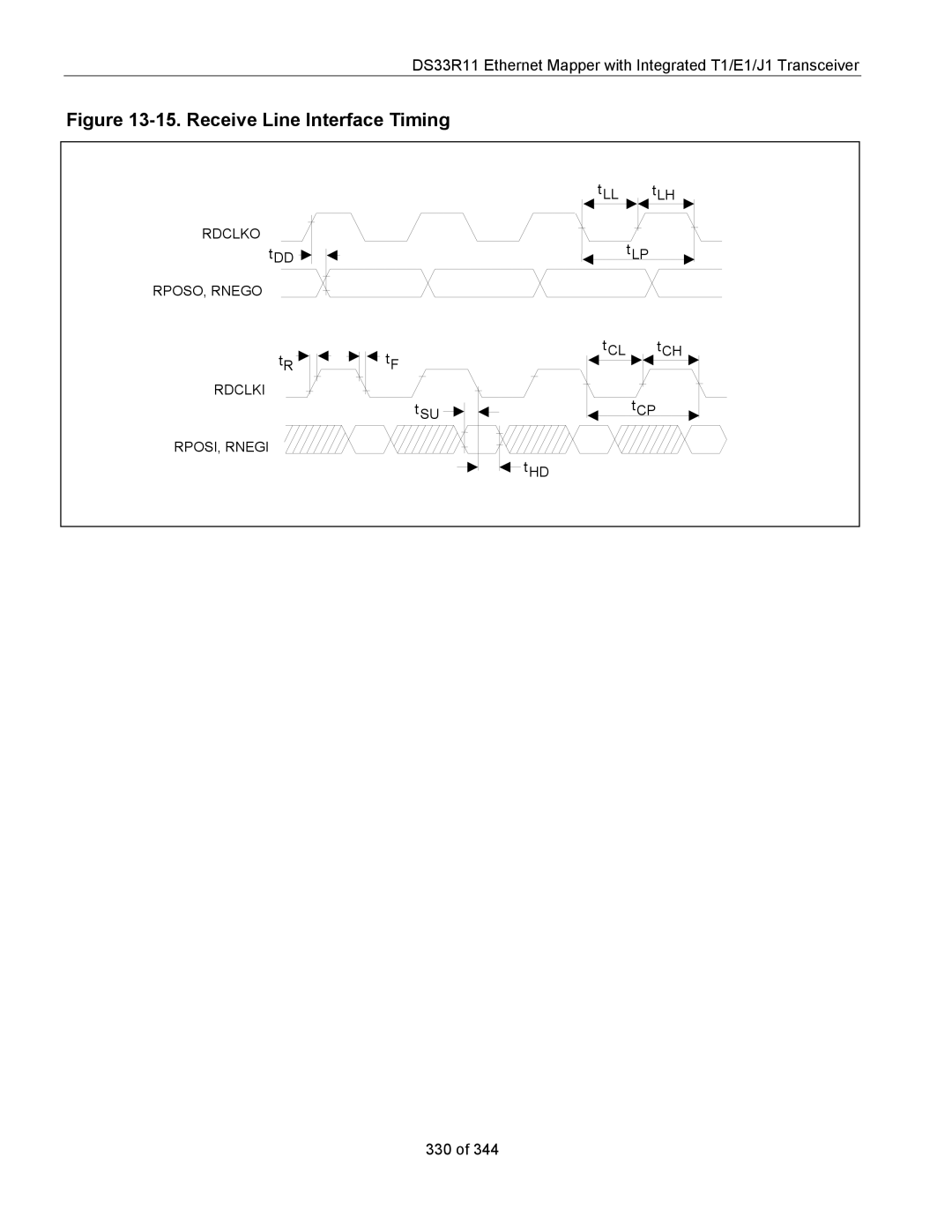
15. Receive Line Interface Timing
16. Receive Timing Delay Rclko to Bpclk
Delay Rclko to Bpclk
Parameter Symbol Conditions MIN TYP E1 MAX Units
TSERI, TSIG, TDATA, TPOSI, Tnegi
17. Transmit-Side Timing
18. Transmit-Side Timing, Elastic Store Enabled
20. Jtag Interface Timing Diagram
Jtag Interface Timing 17. Jtag Interface Timing
Jtag Information
Jtag TAP Controller State Machine Description
Select-IR-Scan
Update-DR
Update-IR
Capture-IR
TAP Controller State Diagram
Instruction Register
Instruction Codes for Ieee 1149.1 Architecture
Instruction Selected Register Instruction Codes
Boundary Scan Register
Jtag ID Codes ID Code Structure
Test Registers
Bypass Register
Jtag Functional Timing
Bypass Idcode State
Package Information
15.1 256-Ball BGA 27mm x 27mm 56-G6004-001
Document Revision History
Revision Description