Pin | Used | Sig. Name | I/O | Active | Note | |
No. | Port | |||||
|
|
|
| |||
|
|
|
|
|
| |
42 | A6 |
|
|
| Address signal | |
|
|
|
|
|
| |
43 | A5 |
|
|
| Address signal | |
|
|
|
|
|
| |
44 | A4 |
|
|
| Address signal | |
|
|
|
|
|
| |
45 | A3 |
|
|
| Address signal | |
|
|
|
|
|
| |
46 | A2 |
|
|
| Address signal | |
|
|
|
|
|
| |
47 | A1 |
|
|
| Address signal | |
|
|
|
|
|
| |
48 | A0 |
|
|
| Address signal | |
|
|
|
|
|
| |
49 | D0 |
|
|
| Data signal | |
|
|
|
|
|
| |
50 | D1 |
|
|
| Data signal | |
|
|
|
|
|
| |
51 | D2 |
|
|
| Data signal | |
|
|
|
|
|
| |
52 | D3 |
|
|
| Data signal | |
|
|
|
|
|
| |
53 | D4 |
|
|
| Data signal | |
|
|
|
|
|
| |
54 | D5 |
|
|
| Data signal | |
|
|
|
|
|
| |
55 | D6 |
|
|
| Data signal | |
|
|
|
|
|
| |
56 | D7 |
|
|
| Data signal | |
|
|
|
|
|
| |
57 | DPFC | O | H | |||
|
|
|
|
|
| |
58 | DRRC | O | H | Transport roller clutch signal | ||
|
|
|
|
|
| |
59 | PS | O | — Not Used | |||
|
|
|
|
|
| |
60 | /RD |
|
|
| ROM READ pin | |
|
|
|
|
|
| |
61 | /WR |
|
|
| Stepping motor data | |
|
|
|
|
| WRITE pin | |
|
|
|
|
|
| |
62 | /AS |
|
|
| Address strobe pin | |
|
|
|
|
| ||
|
|
|
|
|
| |
63 | /CLK |
|
|
| System clock pin | |
|
|
|
|
| ||
|
|
|
|
|
| |
64 | /WAIT |
|
|
| Wait pin | |
|
|
|
|
|
| |
(3) Stepping motor (PAM1, PAM2) drive circuit
The write data is latched by the HC374 at the writing timing of exter- nal address. When the stepping motor output signal
Write address | Data bus | Drive signal | ACT |
|
|
|
|
H'FF80 | D0 | PAM1 A | H |
|
|
|
|
H'FF80 | D1 | PAM1/A | H |
|
|
|
|
H'FF80 | D2 | PAM1 B | H |
|
|
|
|
H'FF80 | D3 | PAM1/B | H |
|
|
|
|
H'FF80 | D4 | PAM2 A | H |
|
|
|
|
H'FF80 | D5 | PAM2/A | H |
|
|
|
|
H'FF80 | D6 | PAM2 B | H |
|
|
|
|
H'FF80 | D7 | PAM2/B | H |
|
|
|
|
*The power source is driven by VB.
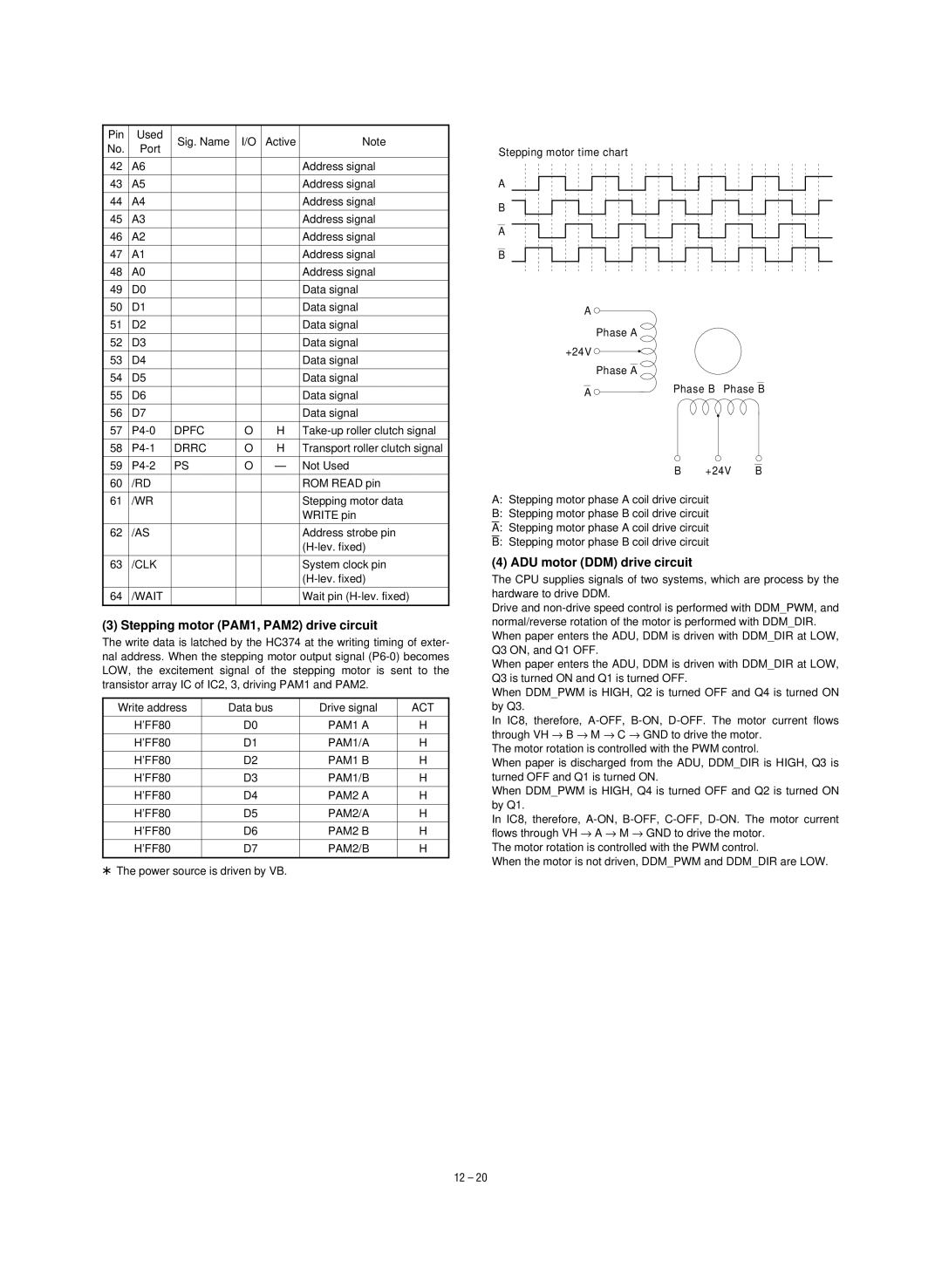
Stepping motor time chart
A
B
A
B
A
Phase A
+24V
Phase A
A | Phase B Phase B |
|
B +24V B
A:Stepping motor phase A coil drive circuit
B:Stepping motor phase B coil drive circuit
A:Stepping motor phase A coil drive circuit
B:Stepping motor phase B coil drive circuit
(4) ADU motor (DDM) drive circuit
The CPU supplies signals of two systems, which are process by the hardware to drive DDM.
Drive and
When paper enters the ADU, DDM is driven with DDM_DIR at LOW, Q3 is turned ON and Q1 is turned OFF.
When DDM_PWM is HIGH, Q2 is turned OFF and Q4 is turned ON by Q3.
In IC8, therefore,
The motor rotation is controlled with the PWM control.
When paper is discharged from the ADU, DDM_DIR is HIGH, Q3 is turned OFF and Q1 is turned ON.
When DDM_PWM is HIGH, Q4 is turned OFF and Q2 is turned ON by Q1.
In IC8, therefore,
The motor rotation is controlled with the PWM control.
When the motor is not driven, DDM_PWM and DDM_DIR are LOW.
12 – 20