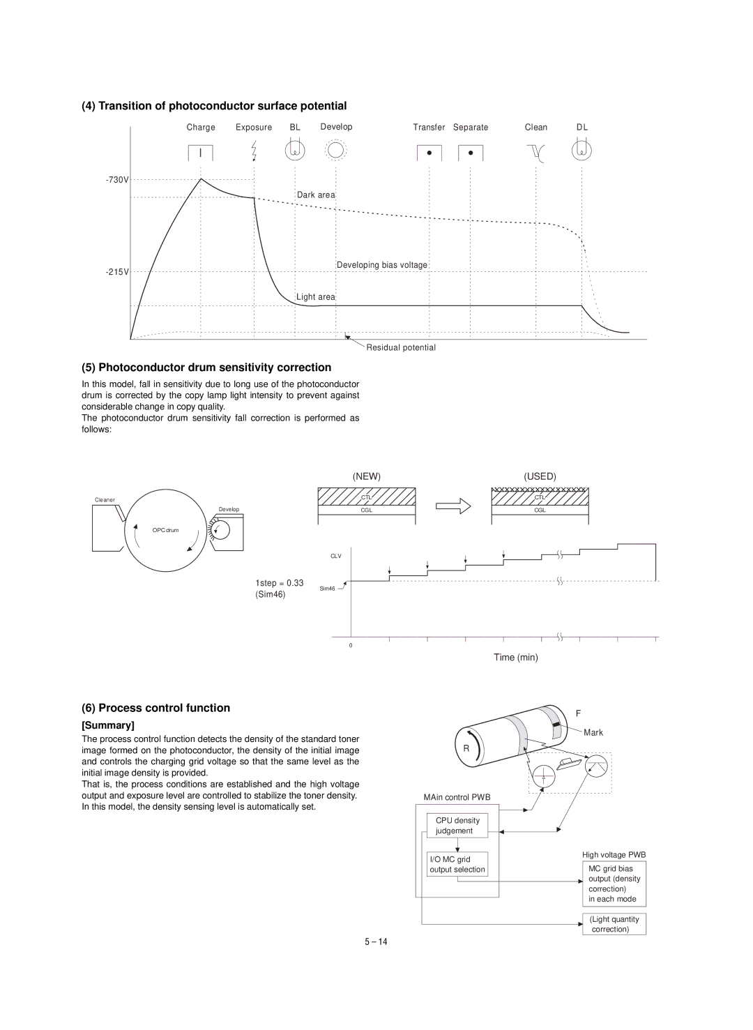
(4) Transition of photoconductor surface potential
Charge | Exposure | BL | Develop | Transfer | Separate | Clean | D L |
|
|
|
|
|
|
| |
|
| Dark area |
|
|
|
| |
|
| Developing bias voltage |
|
|
| ||
|
|
|
|
|
|
| |
|
| Light area |
|
|
|
| |
|
|
|
| Residual potential |
|
|
|
(5) Photoconductor drum sensitivity correction
In this model, fall in sensitivity due to long use of the photoconductor drum is corrected by the copy lamp light intensity to prevent against considerable change in copy quality.
The photoconductor drum sensitivity fall correction is performed as follows:
(NEW) | (USED) |
Cleaner | CTL |
| |
Develop | CGL |
OPC drum |
|
CTL |
CGL |
CLV |
1step = 0.33 |
Sim46 |
(Sim46) |
0 |
Time (min)
(6) Process control function
[Summary]
The process control function detects the density of the standard toner image formed on the photoconductor, the density of the initial image and controls the charging grid voltage so that the same level as the initial image density is provided.
That is, the process conditions are established and the high voltage output and exposure level are controlled to stabilize the toner density. In this model, the density sensing level is automatically set.
F
Mark
R
MAin control PWB
CPU density |
|
judgement |
|
I/O MC grid | High voltage PWB |
| |
output selection | MC grid bias |
| output (density |
| correction) |
| in each mode |
| (Light quantity |
| correction) |
5 – 14