www.ti.com | Peripheral Architecture |
2 Peripheral Architecture
2.1Clock Control
Information related to clock generation and control for the USB peripheral will be added in a future revision of this document. Clocks for USB are generated based on a crystal oscillator on the M24XI and M24XO pins. The oscillator is enabled by bit OSCPDWN of the USBPHY_CTL register in the system module.
2.2Signal Descriptions
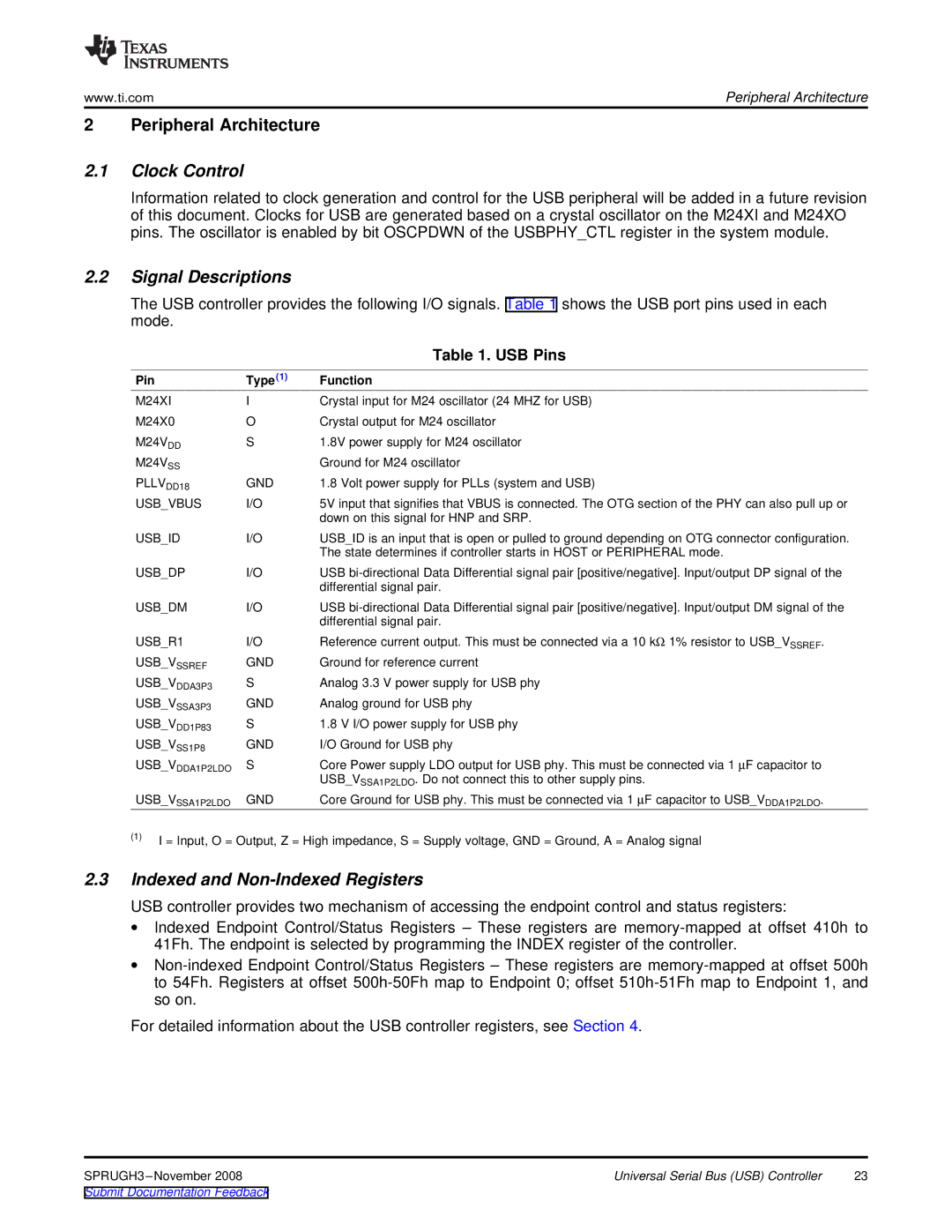
The USB controller provides the following I/O signals. Table 1 shows the USB port pins used in each mode.
|
| Table 1. USB Pins |
Pin | Type(1) | Function |
M24XI | I | Crystal input for M24 oscillator (24 MHZ for USB) |
M24X0 | O | Crystal output for M24 oscillator |
M24VDD | S | 1.8V power supply for M24 oscillator |
M24VSS |
| Ground for M24 oscillator |
PLLVDD18 | GND | 1.8 Volt power supply for PLLs (system and USB) |
USB_VBUS | I/O | 5V input that signifies that VBUS is connected. The OTG section of the PHY can also pull up or |
|
| down on this signal for HNP and SRP. |
USB_ID | I/O | USB_ID is an input that is open or pulled to ground depending on OTG connector configuration. |
|
| The state determines if controller starts in HOST or PERIPHERAL mode. |
USB_DP | I/O | USB |
|
| differential signal pair. |
USB_DM | I/O | USB |
|
| differential signal pair. |
USB_R1 | I/O | Reference current output. This must be connected via a 10 kΩ 1% resistor to USB_VSSREF. |
USB_VSSREF | GND | Ground for reference current |
USB_VDDA3P3 | S | Analog 3.3 V power supply for USB phy |
USB_VSSA3P3 | GND | Analog ground for USB phy |
USB_VDD1P83 | S | 1.8 V I/O power supply for USB phy |
USB_VSS1P8 | GND | I/O Ground for USB phy |
USB_VDDA1P2LDO | S | Core Power supply LDO output for USB phy. This must be connected via 1 μF capacitor to |
|
| USB_VSSA1P2LDO. Do not connect this to other supply pins. |
USB_VSSA1P2LDO | GND | Core Ground for USB phy. This must be connected via 1 μF capacitor to USB_VDDA1P2LDO. |
(1)I = Input, O = Output, Z = High impedance, S = Supply voltage, GND = Ground, A = Analog signal
2.3Indexed and Non-Indexed Registers
USB controller provides two mechanism of accessing the endpoint control and status registers:
∙ Indexed Endpoint Control/Status Registers – These registers are
∙
For detailed information about the USB controller registers, see Section 4.
Universal Serial Bus (USB) Controller | 23 |