Revision/Update Information
Compaq Computer Corporation Shrewsbury, Massachusetts
21264/EV68A Hardware Reference Manual
Table of Contents
Hardware Interface
Cache and External Interfaces
Internal Processor Registers
Privileged Architecture Library Code
Initialization and Configuration
Mffpcr Mtfpcr
Error Detection and Error Handling
Testability and Diagnostics
Electrical Data
Thermal Management
Alpha Instruction Set
21264/EV68A Boundary-Scan Register
21264/EV68A-to-Bcache Pin Interface
Glossary Index
Figures
10-2 Type 2 Heat Sink
Tables
Xiv
VDD Idcpower
Page
Audience
Content
Preface
Documentation Included by Reference
Abbreviations
Terminology and Conventions
For example
W1C
W1S
Addresses
Aligned and Unaligned
Signal Names
Data Units
Do Not Care
External
Undefined
Do not care. a capital X represents any valid value
Page
Introduction
Introduction
Architecture
Architecture
Addressing
Integer Data Types
Floating-Point Data Types
21264/EV68A Microprocessor Features
21264/EV68A Microprocessor Features
21264/EV68A Microprocessor Features
Internal Architecture
Internal Architecture
21264/EV68A Microarchitecture
Virtual Program Counter Logic
Instruction Fetch, Issue, and Retire Unit
21264/EV68A Microarchitecture
21264/EV68A Block Diagram
Branch Predictor
Local Predictor
Global Predictor
Choice Predictor
Instruction-Stream Translation Buffer
Register Rename Maps
Integer Issue Queue
Instruction Fetch Logic
Floating-Point Issue Queue
Hwret
Retire Logic
Integer Execution Unit
Exception and Interrupt Logic
PERR, MINxxx, MAXxxx, UNPKxx, PKxx
Integer Execution Unit-Clusters 0
Floating-Point Execution Unit
10Internal Architecture
21264/EV68A contains two onchip primary-level caches
External Cache and System Interface Unit
Onchip Caches
12Internal Architecture
Memory Reference Unit
Data Cache
Pipeline Organization
Pipeline Organization
Srom Interface
Miss address file MAF Dstream translation buffer DTB
14Internal Architecture
Stage 0 Instruction Fetch
Stage 1 Instruction Slot
Stage 3 Issue
Stage 2 Map
Instruction Issue Rules
Instruction Issue Rules
Pipeline Aborts
Ebox and Fbox pipelines begin execution
Instruction Group Definitions
Instruction Name, Pipeline, and Types
Ebox Slotting
FTOIS, Ftoit
ITOFS, ITOFF, Itoft
Instruction Group Definitions and Pipeline Unit
U U L E L U E E L L E U
Instruction Latencies
Instruction Class Latency in Cycles
Hwmfpr
20Internal Architecture
Minimum Retire Latencies for Instruction Classes
Instruction Retire Rules
Instruction Retire Rules
Retire of Operate Instructions into R31/F31
Retire of Operate Instructions into R31/F31
Floating-Point Divide/Square Root Early Retire
BSR/JSR
Load Instructions to R31 and F31
Load Instructions to R31 and F31
Prefetch with Modify Intent LDS Instruction
Instructions Retired Without Execution
Special Cases of Alpha Instruction Execution
Special Cases of Alpha Instruction Execution
Prefetch, Evict Next LDQ and Hwldq Instructions
Load Hit Speculation
10 Pipeline Timing for Floating-Point Load Instructions
26Internal Architecture
Floating-Point Store Instructions
Cmov Instruction
Memory and I/O Address Space Instructions
Memory and I/O Address Space Instructions
Memory Address Space Load Instructions
2 I/O Address Space Load Instructions
28Internal Architecture
Memory Address Space Store Instructions
Rules for I/O Address Space Load Instruction Data Merging
4 I/O Address Space Store Instructions
Rules for I/O Address Space Store Instruction Data Merging
MAF Memory Address Space Merging Rules
MAF Memory Address Space Merging Rules
Instruction Ordering
Mbox Order Traps
Replay Traps
Replay Traps
12 I/O Write Buffer and the WMB Instruction
Write Buffer and the WMB Instruction
Other Mbox Replay Traps
Memory Barrier MB/WMB/TB Fill Flow
MB Instruction Processing
WMB Instruction Processing
TB Fill Flow
12 TB Fill Flow Example Sequence
13 TB Fill Flow Example Sequence
34Internal Architecture
Performance Measurement Support-Performance Counters
Floating-Point Control Register
Performance Measurement Support-Performance Counters
Floating-point control register Fpcr is shown in Figure
36Internal Architecture
Floating-Point Control Register
14 Floating-Point Control Register Fields
Amask and Implver Instruction Values
Amask and Implver Instruction Values
Design Examples
Design Examples
Amask
Implver
12 Typical Uniprocessor Configuration
Page
Hardware Interface
21264/EV68A Microprocessor Logic Symbol
Hardware Interface
21264/EV68A Microprocessor Logic Symbol
21264/EV68A Microprocessor Logic Symbol
21264/EV68A Signal Names and Functions
21264/EV68A Signal Names and Functions
Signal Pin Types Definitions
21264/EV68A Signal Descriptions
Dcokh
Pllvdd
21264/EV68A Signal Descriptions by Function
TestStatH
SysVref Domain SysAddInL140
Pin Assignments
Pin List Sorted by Signal Name
Pin Assignments
AC1
10Hardware Interface
Pllvdd
AA5
Pin List Sorted by PGA Location
12Hardware Interface
SysDataL28
14Hardware Interface
BcDataH70 SysDataL5
Ground and Power VSS and VDD Pin List
16Hardware Interface
Mechanical Specifications
Mechanical Specifications
18Hardware Interface
21264/EV68A Packaging
21264/EV68A Packaging
21264/EV68A Bottom View Pin Up
Page
Cache and External Interfaces
Cache and External Interfaces
Introduction to the External Interfaces
Introduction to the External Interfaces
System Interface
21264/EV68A System and Bcache Interfaces
Commands and Addresses
Physical Address Considerations
Physical Address Considerations
Second-Level Cache Bcache Interface
ECB I/O
MB/WMB
Physical Address Considerations
Bcache Interface Signals
Bcache Structure
Bcache Structure
System Duplicate Tag Stores
Victim Data Buffer
Cache Coherency
Victim Data Buffer
Cache Coherency Basics
Cache Coherency
Cache Block States
2lists the cache block states supported by the 21264/EV68A
21264/EV68A-Supported Cache Block States
Mands. -4lists these commands
System Responses to 21264/EV68A Commands
Cache Block State Transitions
Cache Block State Transitions
Using SysDc Commands
System Responses to 21264/EV68A Commands and Reactions
12Cache and External Interfaces
Dcache States and Duplicate Tags
14Cache and External Interfaces
Lock Mechanism
Lock Mechanism
Liveness and Fairness
In-Order Processing of LDxL/STxC Instructions
Internal Eviction of LDxL Blocks
16Cache and External Interfaces
System Port
System Port
System Port Pins
System Port Pins
Programming the System Interface Clocks
Programming Values for System Interface Clocks
Program Values for Data-Sample/Drive CSRs
18Cache and External Interfaces
Forwarded Clocks and Frame Clock Ratio
3 21264/EV68A-to-System Commands
Bank Interleave on Cache Block Boundary Mode
Hit Mode
11 Page Hit Mode of Operation
12 21264/EV68A-to-System Command Fields Definitions
12describes the field definitions for Tables 4-10and
4 21264/EV68A-to-System Commands Descriptions
14describes the 21264/EV68A-to-system commands
14 21264/EV68A-to-System Commands Descriptions
13 Maximum Physical Address for Short Bus Format
22Cache and External Interfaces
15 Programming INVALTODIRTYENABLE10
ProbeResponse Commands Command40 =
16 Programming SETDIRTYENABLE20
17 21264/EV68A ProbeResponse Command
24Cache and External Interfaces
18 ProbeResponse Fields Descriptions
SysAck and 21264/EV68A-to-System Commands Flow Control
18describes the ProbeResponse command fields
System-to-21264/EV68A Commands
Probe Commands Four Cycles
19 System-to-21264/EV68A Probe Commands
RVB RPB
20 System-to-21264/EV68A Probe Commands Fields Descriptions
21 lists the data movement selected by Probe43
22lists the next cache block state selected by Probe20
21 Data Movement Selection by Probe43
28Cache and External Interfaces
Data Transfer Commands Two Cycles
23 Data Transfer Command Format
24describes the SysDc40 field
24 SysDc40 Field Description
30Cache and External Interfaces
Data Movement In and Out of the 21264/EV68A
8.1 21264/EV68A Clock Basics
Fast Data Mode
25 Sysclk Cycles Between SysAddOut and SysData
32Cache and External Interfaces
Fast Data Disable Mode
26shows four example configurations and shows their use
26 Cbox CSR SYSDCDELAY40 Examples
27 Four Timing Examples
SysDataInValidL and SysDataOutValidL
SysDataInValidL
34Cache and External Interfaces
SysDataOutValidL
SysFillValidL
36Cache and External Interfaces
Data Wrapping
28 Data Wrapping Rules
30 Wrap Interleave Order
30defines the interleaved scheme for the wrap order
29 System Wrap and Deliver Data
Nonexistent Memory Processing
31defines the wrap order for double-pumped data trans fers
31 Wrap Order for Double-Pumped Data Transfers
38Cache and External Interfaces
21264/EV68A Command NXM Address System/21264/EV68A Response
40Cache and External Interfaces
10.1 21264/EV68A Commands and System Probes
Ordering of System Port Transactions
System Port
Bcache Port
Bcache Port
35 Range of Maximum Bcache Clock Ratios
Bcache Port Pins
36 Bcache Port Pins
Bcache Clocking
44Cache and External Interfaces
Setting the Period of the Cache Clock
37 BCCPUCLKDELAY10 Values
38 BCCLKDELAY10 Values
39 Program Values to Set the Cache Clock Period Single-Data
46Cache and External Interfaces
Bcache Data Read and Tag Read Transactions
Bcache Transactions
41 Data-Sample/Drive Cbox CSRs
Bcache Data Write Transactions
48Cache and External Interfaces
When the ratio is even, bcfrm is equal to the ratio
When the ratio is odd, bcfrm is twice the ratio
For example, in single-data mode
Dual-data mode, bcfrm is twice the ratio
Pin Descriptions
Relationship Between Write-to-Read Bcwrrdbubbles and wrrd
Relationship Between Read-to-Write Bcrdwrbubbles and rdwr
50Cache and External Interfaces
Bcache Control Pins
43 Programming the Bcache Control Pins
44 lists the combination of control pin assertion for
BcAddH234
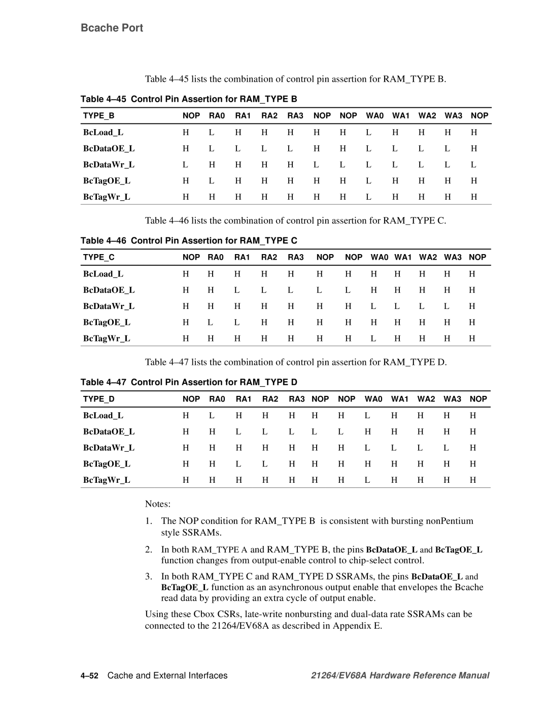
45 Control Pin Assertion for Ramtype B
46 Control Pin Assertion for Ramtype C
47 Control Pin Assertion for Ramtype D
52Cache and External Interfaces
BcDataInClkH and BcTagInClkH
Bcache Banking
Disabling the Bcache for Debugging
54Cache and External Interfaces
Interrupts
Interrupts
Internal Processor Registers
Internal Processor Registers
Mbox IPRs
Ebox IPRs
Ebox IPRs
Cycle Counter Register CC
Cycle Counter Control Register Ccctl
Virtual Address Register VA
Virtual Address Control Register Vactl
2describes the Ccctl register fields
Cycle Counter Control Register Fields Description
Virtual Address Format Register Vaform
3describes the virtual address control register fields
Virtual Address Control Register Fields Description
VAFORM32
Ibox IPRs
Ibox IPRs
ITB Tag Array Write Register Itbtag
ITB PTE Array Write Register Itbpte
ITB Invalidate Single Register Itbis
ITB Invalidate All Process ASM=0 Register Itbiap
ITB Invalidate All Register Itbia
ProfileMe PC Register Pmpc
Exception Address Register Excaddr
4describes the ProfileMe PC register fields
ProfileMe PC Fields Description
Interrupt Enable and Current Processor Mode Register Iercm
Instruction Virtual Address Format Register Ivaform
10Internal Processor Registers
Software Interrupt Request Register Sirr
Iercm Register Fields Description
Software Interrupt Request Register Fields Description
Interrupt Summary Register Isum
6describes the software interrupt request register fields
Hardware Interrupt Clear Register Hwintclr
7describes the interrupt summary register fields
Interrupt Summary Register Fields Description
12Internal Processor Registers
Exception Summary Register Excsum
8describes the hardware interrupt clear register fields
Hardware Interrupt Clear Register Fields Description
Mchkd W1C
14Internal Processor Registers
9describes the exception summary register fields
Exception Summary Register Fields Description
PAL Base Register Palbase
Ibox Control Register Ictl
10describes the PAL base register fields
10 PAL Base Register Fields Description
16Internal Processor Registers
11describes the Ibox control register fields
11 Ibox Control Register Fields Description
Singleissueh
STWAIT64K
PCT1EN
PCT0EN
18Internal Processor Registers
Ibox Status Register Istat
Spce
12describes the Ibox status register fields
12 Ibox Status Register Fields Description
MIS
TRP
20Internal Processor Registers
Sleep Mode Register Sleep
Icache Flush Register Icflush
Icache Flush ASM Register Icflushasm
Clear Virtual-to-Physical Map Register Clrmap
22Internal Processor Registers
14describes the process context register fields
14 Process Context Register Fields Description
15 Performance Counter Control Register Fields Description
Performance Counter Control Register Pctrctl
15describes the performance counter control register fields
Pctxppce
Pmstalled
Pmkilledbm
SL0
Mbox IPRs
Mbox IPRs
DTB Tag Array Write Registers 0 and 1 DTBTAG0, DTBTAG1
16 Performance Counter Control Register Input Select Fields
DTB Alternate Processor Mode Register Dtbaltmode
17 DTB Alternate Processor Mode Register Fields Description
DTB PTE Array Write Registers 0 and 1 DTBPTE0, DTBPTE1
17describes the Dtbaltmode register fields
Dstream TB Invalidate All Process ASM=0 Register Dtbiap
Dstream TB Invalidate All Register Dtbia
Dstream TB Invalidate Single Registers 0 and 1 DTBIS0,1
ALTMODE10
Dstream TB Address Space Number Registers 0 and 1 DTBASN0,1
Memory Management Status Register Mmstat
18describes the memory management status register fields
18 Memory Management Status Register Fields Description
ACV
Mbox Control Register Mctl
For
Erences to superpages result in access violations
Dcache Control Register Dcctl
19describes the Mbox control register fields
19 Mbox Control Register Fields Description
20 Dcache Control Register Fields Description
Dcache Status Register Dcstat
20describes the Dcache control register fields
Cbox CSRs and IPRs
Cbox CSRs and IPRs
21describes the Dcache status register fields
21 Dcache Status Register Fields Description
Cbox Data Register Cdata
Cbox Shift Register Cshft
Cbox Writeonce Chain Description
22 describes the Cbox data register fields
24 Cbox Writeonce Chain Order
34Internal Processor Registers
BCWRRDBUBBLES03
Mboxbcprbstall BCLATDATAPATTERN031 BCLATTAGPATTERN023
36Internal Processor Registers
SYSCLKDELAY10
Cbox Writemany Chain Description
38Internal Processor Registers
25 Cbox Writemany Chain Order
40Internal Processor Registers
Cbox Read Register IPR Description
26 Cbox Read IPR Fields Description
0 1 1 Dstreammemerr
0 1 1 Istreammemerr
Privileged Architecture Library Code
Privileged Architecture Library Code
PALcode Description
PALmode Environment
PALmode Environment
Required PALcode Function Codes
Opcodes Reserved for PALcode
Required PALcode Function Codes
Hwld Instruction
Opcodes Reserved for PALcode
Hwst Instruction
3describes the Hwld instruction fields
Hwld Instruction Fields Descriptions
Hwst Instruction Fields Descriptions
Hwret Instruction
4describes the Hwst instruction fields
Hwmfpr and Hwmtpr Instructions
5describes the Hwret instruction fields
Hwret Instruction Fields Descriptions
Hint
Internal Processor Register Access Mechanisms
Internal Processor Register Access Mechanisms
6describes the Hwmfpr and Hwmtpr instructions fields
Hwmfpr and Hwmtpr Instructions Fields Descriptions
IPR Scoreboard Bits
Hardware Structure of Explicitly Written IPRs
Paired Instruction Fetch Order
IPR Access Ordering
Hardware Structure of Implicitly Written IPRs
10Privileged Architecture Library Code
PALshadow Registers
PALshadow Registers
PALcode Emulation of the Fpcr
PALcode Entry Points
PALcode Entry Points
PALcode Exception Entry Points
PALcode Exception Entry Locations
Translation Buffer TB Fill Flows
Translation Buffer TB Fill Flows
DTB Fill
14Privileged Architecture Library Code
Wr PTE LD-PTE, write TB
Wr Data
Tb miss
ITB Fill
16Privileged Architecture Library Code
Performance Counter Support
Performance Counter Support
General Precautions
Aggregate Mode Programming Guidelines
Aggregate Mode Precautions
IPRs Used for Performance Counter Support
10 Aggregate Mode Returned IPR Contents
Operation
Pctrctl SL0
SL1
This input counts Mbox replay traps
ProfileMe Mode Programming Guidelines
11shows the counter modes that are used with Aggregate mode
12 Cmov Decomposed
13 ProfileMe Mode Returned IPR Contents
22Privileged Architecture Library Code
ProfileMe Counting Mode Description Cycle counting
Inum retire delay cycles
14shows the counter modes that are used with ProfileMe mode
Counter Modes for ProfileMe Mode
14 ProfileMe Mode Pctrctl Input Select Fields
24Privileged Architecture Library Code
Initialization and Configuration
Power-Up Reset Flow and the ResetL and Dcokh Pins
21264/EV68A Reset State Machine Major Operations
Initialization and Configuration
Power-Up Reset Flow and the ResetL and Dcokh Pins
Constraints
Power Sequencing and Reset State for Signal Pins
Signal Pin Reset State
Clock Forwarding and System Clock Ratio Configuration
Pllvdd
Pin Signal Names and Initialization State
PLL
PLL Ramp Up
BiST and Srom Load and the TestStatH Pin
EV68A
Clock Forward Reset and System Interface Initialization
Power-Up Flow Signals and Their Constraints
Effect on IPRs After Fault Reset
Fault Reset Flow
Fault Reset Flow
Energy Star Certification and Sleep Mode Flow
Energy Star Certification and Sleep Mode Flow
Effect on IPRs After Transition Through Sleep Mode
10Initialization and Configuration
Warm Reset Flow
Warm Reset Flow
Signals and Constraints for the Sleep Mode Sequence
Effect on IPRs After Warm Reset
Initialization Mode Processing
12Initialization and Configuration
Array Initialization
Array Initialization
Initialization Mode Processing
Evictenable BCWRTSTS30 Bcbankenable
Internal Processor Register Power-Up Reset State
10 Internal Processor Registers at Power-Up Reset State
14Initialization and Configuration
External Interface Initialization
Internal Processor Register Power-Up Reset State
Ieee 1149.1 Test Port Reset
Reset State Machine
Ieee 1149.1 Test Port Reset
16Initialization and Configuration
Reset State Machine
11 21264/EV68A Reset State Machine State Descriptions
18Initialization and Configuration
Phase-Lock Loop PLL Functional Description
Phase-Lock Loop PLL Functional Description
Differential Reference Clocks
PLL Output Clocks
Power-Up/Reset Clocking
20Initialization and Configuration
Error Detection and Error Handling
Error Detection and Error Handling
21264/EV68A Error Detection Mechanisms
Data Error Correction Code
Icache Data or Tag Parity Error
Dcache Tag Parity Error
Data Error Correction Code
Load Instruction
Dcache Data Single-Bit Correctable ECC Error
Dcache Data Single-Bit Correctable ECC Error
Dcache Store Second Error
Dcache Duplicate Tag Parity Error
Dcache Store Second Error
Store Instruction Quadword or Smaller
Bcache Tag Parity Error
Bcache Data Single-Bit Correctable ECC Error
Bcache Tag Parity Error
Controlling Bcache Block Parity Calculation
Bcache Data Single-Bit Correctable ECC Error
Dcache Fill from Bcache
Memory/System Port Single-Bit Data Correctable ECC Error
Memory/System Port Single-Bit Data Correctable ECC Error
Bcache Victim Read
Icache Fill from Memory
Dcache Fill from Memory
Bcache Data Single-Bit Correctable ECC Error on a Probe
Bcache Data Single-Bit Correctable ECC Error on a Probe
Double-Bit Fill Errors
Error Case Summary
Error Case Summary
3summarizes the various error cases and their ramifications
Section D.36
Mchk Cstatistreammemerr
Cstatdstreammemerr
CRD Cstatprobebcerr
Mchk Cstatistreambcdbl
Page
Electrical Characteristics
Electrical Data
1lists the maximum electrical ratings for the 21264/EV68A
Maximum Electrical Ratings
DC Characteristics
DC Characteristics
Signal Types
Idcpower
VDD Idcpower
Input DC Reference Pin Idcref
Input Differential Amplifier Receiver IDA
Input Differential Amplifier Clock Receiver Idaclk
Pin Type Open-Drain Driver for Test Pins Oodtp
Pin Type Open-Drain Output Driver OOD
IOZ
Codtp
11 Push-Pull Output Driver OPP
12 Push-Pull Output Clock Driver Oppclk
AC Test Conditions
AC Characteristics
AC Characteristics
13 AC Specifications
TSU1 TDH2
Dcokh
AC Characteristics
Page
Operating Temperature
Operating Temperature at Heat Sink Center Tc
Thermal Management
That causes thermal failure
10-2Thermal Management
Operating Temperature
Θca at Various Airflows for 21264/EV68A
Heat Sink Specifications
Heat Sink Specifications
Type 2 Heat Sink
10-4Thermal Management
Type 3 Heat Sink
10-6Thermal Management
Thermal Design Considerations
Thermal Design Considerations
Testability and Diagnostics
Test Pins
Dedicated Test Port Pins
Testability and Diagnostics
SROM/Serial Diagnostic Terminal Port
SROM/Serial Diagnostic Terminal Port
11-2Testability and Diagnostics
Srom Load Operation
Ieee 1149.1 Instructions and Opcodes
Ieee 1149.1 Port
Ieee 1149.1 Port
11-4Testability and Diagnostics
TestStatH Pin
TestStatH Pin
TAP Controller State Machine
Power-Up Self-Test and Initialization
Power-Up Self-Test and Initialization
Built-in Self-Test
Srom Initialization
11-6Testability and Diagnostics
Serial Instruction Cache Load Operation
References
See Appendix B for a listing of the Boundary-Scan Register
Icache Bit Fields in an Srom Line
Page
Alpha Instruction Set
Alpha Instruction Summary
Table A-1 Instruction Format and Opcode Notation
Alpha Instruction Set A-1
Alpha Instruction Summary
Mbr Branch to subroutine
Pcd Trap to PALcode
Opr 11.24 Cmove if = zero
Opr 11.46 Cmove if ≥ zero
15.0AF Convert Gfloating to quadword
17.010 Convert longword to quadword
15.0BC Convert quadword to Ffloating
15.0BE Convert quadword to Gfloating
17.02F Fcmove if zero
17.02E Fcmove if ≤ zero
17.02C Fcmove if zero
17.02B Fcmove if ≠ zero
Opr 13.40 Multiply longword with integer overflow enable
Opr 13.60 Multiply quadword with integer overflow enable
Opr 1C.31 Pixel error
Mem Load Sfloating
Opr 1C.36 Pack words to bytes Mfc 18.E000 Read and clear
Mbr 1A.2 Return from subroutine
Mfc 18.C000 Read process cycle counter 18.F000 Read and set
Opr 10.02 Scaled add longword by
Opcodes Reserved for Compaq
Reserved Opcodes
Reserved Opcodes
Opcodes Reserved for PALcode
Ieee Floating-Point Instructions
Ieee Floating-Point Instructions
08B 00B 04B
18B 10B 14B
02B 06B
12B 16B
VAX Floating-Point Instructions
VAX Floating-Point Instructions
Independent Floating-Point Instructions
Opcode Summary
Opcode Summary
Mem Table A-9explains the symbols used in Table A-8
Mem Res
Ieee floating-point instruction opcodes
Floating-point operate instruction opcodes
14Alpha Instruction Set
Ieee Floating-Point Conformance
Ieee Floating-Point Conformance
Table A-11 Exceptional Input and Output Conditions
Alpha Instruction Set A-15
16Alpha Instruction Set
Alpha Instruction Set A-17
Cmpteq Cmptun Input
Cmptlt Cmptle Input
Fbeq Fbne Fblt Fble Fbgt Fbge LDS LDT STS STT Cpys Cpysn
21264/EV68A Boundary-Scan Register
Boundary-Scan Register
Boundary-Scan Register
Pllvdd
21264/EV68A Boundary-Scan Register B-3
421264/EV68A Boundary-Scan Register
21264/EV68A Boundary-Scan Register B-5
621264/EV68A Boundary-Scan Register
21264/EV68A Boundary-Scan Register B-7
821264/EV68A Boundary-Scan Register
21264/EV68A Boundary-Scan Register B-9
1021264/EV68A Boundary-Scan Register
21264/EV68A Boundary-Scan Register B-11
1221264/EV68A Boundary-Scan Register
Serial Icache Load Predecode Values
Serial Icache Load Predecode Values C-1
Page
PALcode Restrictions and Guidelines
PALcode Restrictions and Guidelines D-1
2PALcode Restrictions and Guidelines
PALcode Restrictions and Guidelines D-3
4PALcode Restrictions and Guidelines
PALcode Restrictions and Guidelines D-5
Initwritemany
6PALcode Restrictions and Guidelines
PALcode Restrictions and Guidelines D-7
8PALcode Restrictions and Guidelines
Restriction 7 Replay Trap, Interrupt Code Sequence, and STF
PALcode Restrictions and Guidelines D-9
Restriction 10 Duplicate IPR Mode Bits
Restriction 9 PALmode Istream Address Ranges
Restriction 9 PALmode Istream Address Ranges
10PALcode Restrictions and Guidelines
Restriction 11 Ibox IPR Update Synchronization
Restriction 11 Ibox IPR Update Synchronization
Restriction 13 DTB Fill Flow Collision
Restriction 14 Hwret
Guideline 20 Ictlsbe Stream Buffer Enable
Guideline 16 JSR-BAD VA
Restriction 21 HWRET/STALL After Hwmtpr ASN0/ASN1
Guideline 16 JSR-BAD VA
PALcode Restrictions and Guidelines D-13
Restriction 22 HWRET/STALL After Hwmtpr IS0/IS1
Restriction 22 HWRET/STALL After Hwmtpr IS0/IS1
Restriction 25 Hwmtpr Itbia After Reset
Guideline 26 Conditional Branches in PALcode
Restriction 24 HWRET/STALL After Hwmtpr ICFLUSH, Icflushasm
14PALcode Restrictions and Guidelines
PALcode Restrictions and Guidelines D-15
Guideline 29 JSR, JMP, RET, and Jsrcor in PALcode
Restriction 30 Hwmtpr and Hwmfpr to the Cbox CSR
Restriction 30 Hwmtpr and Hwmfpr to the Cbox CSR
16PALcode Restrictions and Guidelines
Restriction 31 ICTLVA48 Update
Restriction 32 Pctrctl Update
Restriction 31 ICTLVA48 Update
PALcode Restrictions and Guidelines D-17
Guideline 35 Hwintclr Update
Restriction 33 Hwld Physical/Lock Use
Restriction 36 Updating Ictlsde
Restriction 37 Updating VACTLVA48
Restriction 40 Scrubbing a Single-Bit Error
PALcode Restrictions and Guidelines D-19
Restriction 40 Scrubbing a Single-Bit Error
20PALcode Restrictions and Guidelines
PALcode Restrictions and Guidelines D-21
Restriction 42 Updating VACTL, CCCTL, or CC IPRs
Restriction 43 No Trappable Instructions Along with
Restriction 47 Cache Eviction for Single-Bit Cache Errors
22PALcode Restrictions and Guidelines
Restriction 47 Cache Eviction for Single-Bit Cache Errors
PALcode Restrictions and Guidelines D-23
24PALcode Restrictions and Guidelines
Table E-1 Bcache Forwarding Clock Pin Groupings
21264/EV68A-to-Bcache Pin Interface
Forwarding Clock Pin Groupings
Late-Write Non-Bursting SSRAMs
Late-Write Non-Bursting SSRAMs
Data Pin Usage
Tag Pin Usage
Table E-4 Dual-Data Rate Ssram Data Pin Usage
Dual-Data Rate SSRAMs
Dual-Data Rate SSRAMs
421264/EV68A-to-Bcache Pin Interface
Trstl
Table E-5 Dual-Data Rate Ssram Tag Pin Usage
21264/EV68A-to-Bcache Pin Interface E-5
Page
Glossary
BIU
BSR
Cisc
Cmos
CPI
CPU
CSR
DMA
Dram
DTB
DTL
Feprom
FET
FEU
Fpga
Gclk
IDU
Iowb
Ipga
ITB
Jfet
MAF
MBO
MBZ
Mips
MSI
Naturally Aligned
Nmos
Nvram
PAL
PGA
PLA
Plcc
Pqfp
Prom
RAM
RAS
Risc
ROM
RTL
SAM
Sdram
Simm
SIP
Sipp
Stram
TTL
Uart
Unaligned
Unpredictable
Uvprom
VAF
VDF
WAR
Writeblock
Index
Numerics
Index-2
Index-3
Index-4
ECC
Index-6
Index-7
Index-8
Index-9
Index-10
Index-11
Index-12