HARDWARE DESIGN
Secondly, a multiplexed system is necessarily small- usually less than 15 components- due to the limited drive capability of the MOS parts which directly drive the bus.
Larger iAPX 88 systems will normally use a demultiplexed and buffered bus configura- tion, (Fig.
Memory and Peripheral Interface
The 8088 uses address, data and control information to control and communicate with system memory and peripheral compo- nents. Some components connect directly to the multiplexed Address/Data Bus, while others have separate address and data pins and must connect to a demultiplexed bus. Some interfacing methods for both multi- plexed and demultiplexed busses follow.
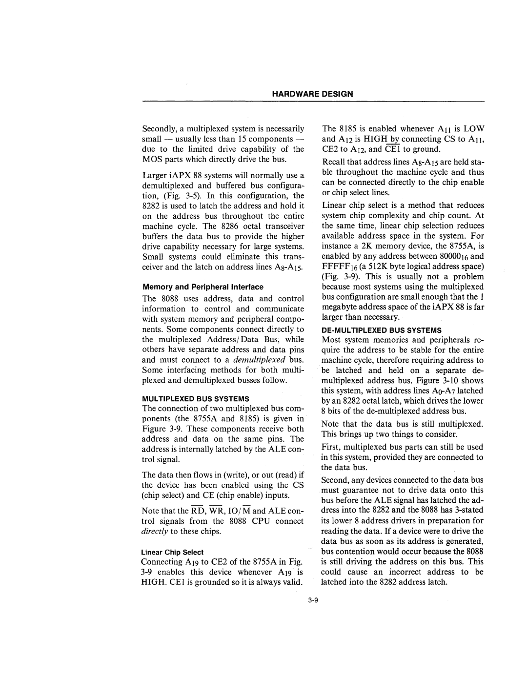
MULTIPLEXED BUS SYSTEMS
The connection of two multiplexed bus com- ponents (the 8755A and 8185) is given in Figure
The data then flows in (write), or out (read) if the device has been enabled using the CS (chip select) and CE (chip enable) inputs.
Note that the RD, WR, IO/M and ALE con- trol signals from the 8088 CPU connect directly to these chips.
Linear Chip Select
Connecting A19 to CE2 of the 8755A in Fig.
The 8185 is enabled whenever All is LOW and A12 is HIGH by connecting CS to All, CE2 to Al2, and CEI to ground.
Recall that address lines
Linear chip select is a method that reduces system chip complexity and chip count. At the same time, linear chip selection reduces available address space in the system. For instance a 2K memory device, the 8755A, is enabled by any address between 8000016 and FFFFF16 (a 512K byte logical address space) (Fig.
Most system memories and peripherals re- quire the address to be stable for the entire machine cycle, therefore requiring address to be latched and held on a separate de- multiplexed address bus. Figure
Note that the data bus is still multiplexed. This brings up two things to consider.
First, multiplexed bus parts can still be used in this system, provided they are connected to the data bus.
Second, any devices connected to the data bus must guarantee not to drive data onto this bus before the ALE signal has latched the ad- dress into the 8282 and the 8088 has