HARDWARE DESIGN
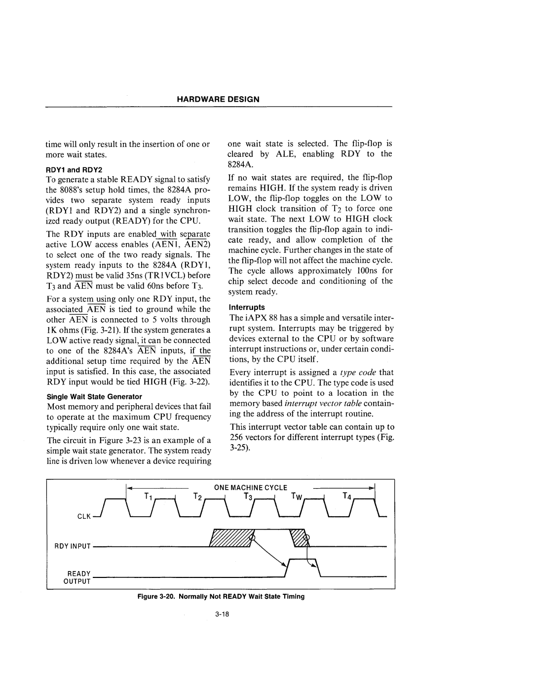
time will only result in the insertion of one or more wait states.
RDY1 and RDY2
one wait state is selected. The
To generate a stable READY signal to satisfy the 8088's setup hold times, the 8284A pro- vides two separate system ready inputs (RDYI and RDY2) and a single synchron- ized ready output (READY) for the CPU.
The RDY inputs are enabled with separate active LOW access enables (AENI, AEN2) to select one of the two ready signals. The system ready inputs to the 8284A (RDYI, RDY2) must be valid 35ns (TRI VCL) before T3 and AEN must be valid 60ns before T3.
For a system using only one RDY input, the associated AEN is tied to ground while the other AEN is connected to 5 volts through lK ohms (Fig.
Single Wait State Generator
Most memory and peripheral devices that fail to operate at the maximum CPU frequency typically require only one wait state.
The circuit in Figure
eLK
If no wait states are required, the
Interrupts
The iAPX 88 has a simple and versatile inter- rupt system. Interrupts may be triggered by devices external to the CPU or by software interrupt instructions or, under certain condi- tions, by the CPU itself.
Every interrupt is assigned a type code that identifies it to the CPU. The type code is used by the CPU to point to a location in the memory based interrupt vector table contain- ing the address of the interrupt routine.
This interrupt vector table can contain up to 256 vectors for different interrupt types (Fig.
RDYINPUT~~
READY _______________________~ ~,____________