CHAPTER 3
HARDWARE DESIGN
INTRODUCTION
This chapter discusses the hardware design of iAPX 88 systems. First, the pins and signals of the 8088 CPU are functionally described for simple, but powerful iAPX 88 systems.
The timings of 8088 signals are explained, and how they cleanly interface the 8088 CPU with the rest of the system.
Other parts of the iAPX 88 system are dis- cussed including, the clock generator, reset and wait state circuits.
Interrupt handling follows, leading into a description of maximum mode iAPX 88 systems.
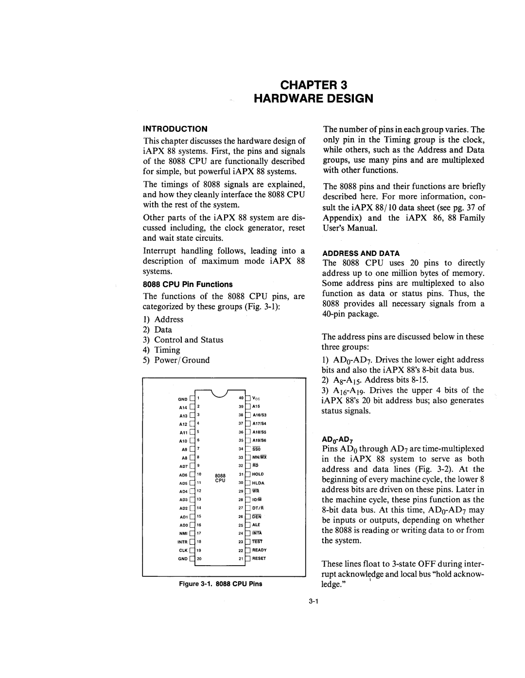
8088 CPU Pin Functions
The functions of the 8088 CPU pins, are categorized by these groups (Fig.
1)Address
2)Data
3)Control and Status
4)Timing
5)Power/Ground
GND |
|
|
|
A14 |
|
|
|
A13 |
| 38 | A18/S3 |
A12 |
| 37 | A171S4 |
A11 |
| 36 | A181S5 |
A10 |
| 35 | A19/S6 |
A9 |
| 34 | SSO |
A8 |
| 33 | MN/!.lX |
AD7 |
| 32 | iiii |
AD6 | 8088 | 31 | HOLD |
| CPU | 30 | HLDA |
|
| ||
|
| 29 | WR |
|
| 28 | 101M |
|
| 27 | DTti'! |
|
| 26 | DEN |
|
| 25 | ALE |
|
| 24 | iNTA |
INTR |
| 23 | TEST |
|
| 22 | READY |
|
| 21 | RESET |
The number of pins in each group varies. The only pin in the Timing group is the clock, while others, such as the Address and Data groups, use many pins and are multiplexed with other functions.
The 8088 pins and their functions are briefly described here. For more information, con- sult the iAPX 88/10 data sheet (see pg. 37 of Appendix) and the iAPX 86, 88 Family User's Manual.
ADDRESS AND DATA
The 8088 CPU uses 20 pins to directly address up to one million bytes of memory. Some address pins are multiplexed to also function as data or status pins. Thus, the 8088 provides all necessary signals from a
The address pins are discussed below in these three groups:
1)
2)
3)
Pins ADo through AD7 are
These lines float to
Figure 3-1. 8088 CPU Pins
ledge."
\