HARDWARE DESIGN
drive specified to drive 2.0mA and 100pF, a system with 5 peripheral components and 10 memory components would overload the bus.
The 8282
Note that adding these latches and transceiv- ers increases the chip count and adds propagation delays (25ns for the 8283 and 8287 and 35ns for the 8282 and 8286) that subtract from the read or write access time of the system's memory and peripheral devices. For complete specifications of the 8283/8282 and 8286/8287 see the data sheets in the Appendix.
Memory Operands
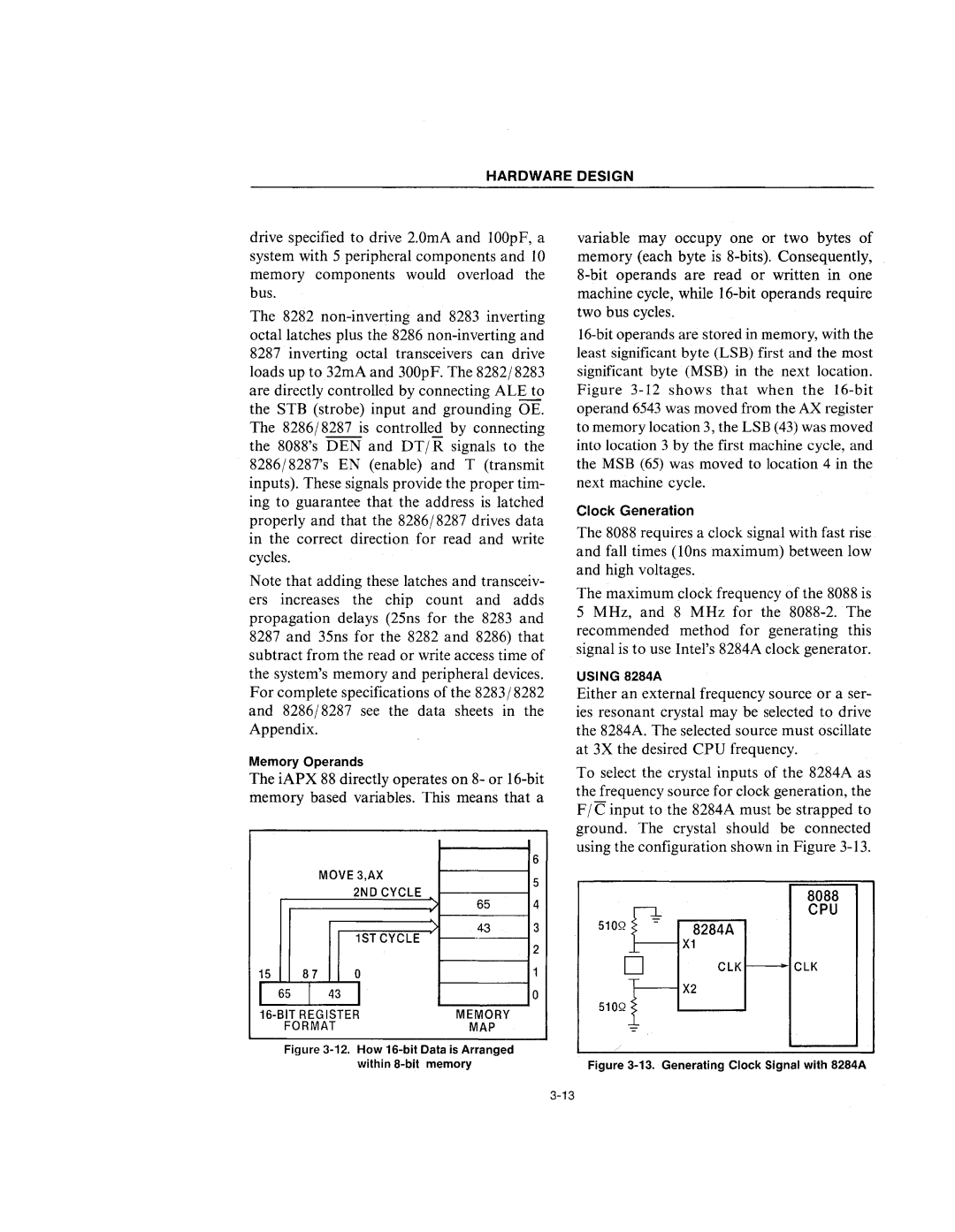
The iAPX 88 directly operates on 8- or
|
|
|
| 6 |
| MOVE 3,AX |
| 5 | |
|
| 2ND CYCLE |
| |
|
| 65 | 4 | |
|
|
| ||
|
| 1ST CYCLE | 3 | |
|
|
|
| 2 |
15 | 87 | 0 |
|
|
I | 65 I 43 | I |
| o |
MEMORY |
| |||
| FORMAT |
| MAP |
|
Figure 3-12. How 16-bit Data is Arranged within 8-bit memory
variable may occupy one or two bytes of memory (each byte is
Clock Generation
The 8088 requires a clock signal with fast rise and fall times (lOns maximum) between low and high voltages.
The maximum clock frequency of the 8088 is 5 MHz, and 8 MHz for the
USING 8284A
Either an external frequency source or a ser- ies resonant crystal may be selected to drive the 8284A. The selected source must oscillate at 3X the desired CPU frequency.
To select the crystal inputs of the 8284A as the frequency source for clock generation, the F / C input to the 8284A must be strapped to ground. The crystal should be connected using the configuration shown in Figure
|
| 8088 | |
510Q | CPU | ||
8284A | |||
|
t
0 ClK ClK
X2
510Q
/