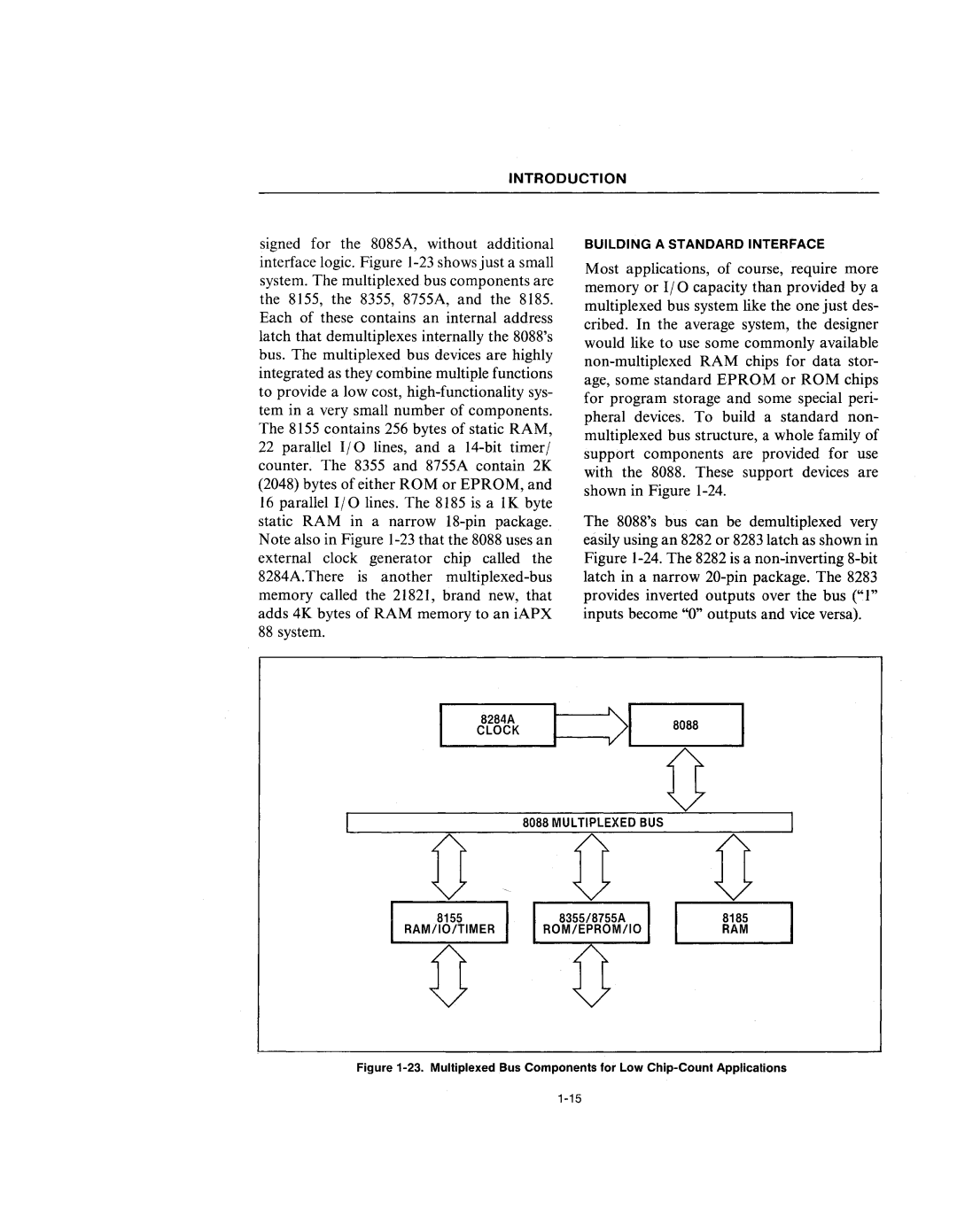
signed for the 8085A, without additional interface logic. Figure 1-23 shows just a small system. The multiplexed bus components are the 8155, the 8355, 8755A, and the 8185. Each of these contains an internal address latch that demultiplexes internally the 8088's bus. The multiplexed bus devices are highly integrated as they combine multiple functions to provide a low cost, high-functionality sys- tem in a very small number of components. The 8155 contains 256 bytes of static RAM, 22 parallel I/O lines, and a 14-bit timer/ counter. The 8355 and 8755A contain 2K (2048) bytes of either ROM or EPROM, and 16 parallel I/O lines. The 8185 is a lK byte static RAM in a narrow 18-pin package. Note also in Figure 1-23 that the 8088 uses an external clock generator chip called the 8284A.There is another multiplexed-bus memory called the 21821, brand new, that adds 4K bytes of RAM memory to an iAPX 88 system.
BUILDING A STANDARD INTERFACE
Most applications, of course, require more memory or I/O capacity than provided by a multiplexed bus system like the one just des- cribed. In the average system, the designer would like to use some commonly available non-multiplexed RAM chips for data stor- age, some standard EPROM or ROM chips for program storage and some special peri- pheral devices. To build a standard non- multiplexed bus structure, a whole family of support components are provided for use with the 8088. These support devices are shown in Figure 1-24.
The 8088's bus can be demultiplexed very easily using an 8282 or 8283 latch as shown in Figure 1-24. The 8282 is a non-inverting 8-bit latch in a narrow 20-pin package. The 8283 provides inverted outputs over the bus ("1" inputs become "0" outputs and vice versa).
L-__C:\:2~~~~\~~j-____:>1L____8~0~88____~
D
8088 MULTIPLEXED BUS
D D
8185
RAM
Figure 1-23. Multiplexed Bus Components for Low Chip-Count Applications