IAPX
Inter
Intel Corporation
About this Book
Page
Table of Contents
List of Figures
List of Figures
IAPX 88 VS. Zilog Z8D
Introduction To
Page
Chapter Introduction
Execution ~STRUCTION BUS
Bus Interface and Execution Units Work in Parallel
~~~11~~ks
Control Registers
Cal address Fig
Result is always 20-bits ofphysical address
13. Process Relocation
Displacement = 12 Wage Code Index
Instruction SET
Powerful String Processing
Conditional Transfers
Interfacing the 8088 is Easy Flexible
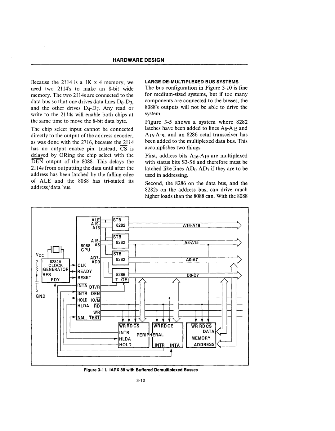
Using Special Multiplexed Bus Parts
\2~~~~\~~j-1L8~0~88~
To,ITovide extra drive capability for the data
IAPX 88 Performance is Cost Effective
Processor
Introduction Review
IAPX 188 CPU
Interrupt Controller
IAPX 188 CPU CPU Internal Registers
IAPX 88 Architecture Instructions
Page
Chapter
Architecture and Instructions
Data Registers Pointer and Index Registers
Flag Register File
Addressing Modes
==~TA~~=J
Direct Addressing
Fffffh
·--- 16 BITs----I.~1
Organization of the Instruction SET
Accumulator-Specific Transfers
Addition
Logic Instructions
Five primitive string oper~tions are provided
Body of this loop requires seven bytes of code
NMI
Instruction Timings
Assembly Language PROGRAMMING1
~g~~CE TRANSLATOR~g~bEECT
Inanqout Segment
MY Data Segment
Summary
Inandout Segment
Equal DB ?
INC CX increment CX
AL,PORTVAL OUT Portval and OFEH,AL
Assembler will assemble
Some examples are
Thing
Allzero DB 6 DUP
Dontcare DB ?,?,?,?,?,?,?,?
Then we could name first the byte in the word as follows
Segment Ends Assume
Mydata Segment Ends Myextra Alpha Beta Gamma Mystack
BL,X
Assume Dsnothing Cycle INC OLD~BYTE
Near and Far
Retstart
Cycle NIL INC AX
MOV AX,BX SI
Cmps BETA,ALPHA Scas Alpha Lods Alpha Stos Beta
Add two unpacked BCD Ascii strings together
Move 50 bytes between two overlapping strings
14. ASM-86 Reserved Words
14. ASM 86 Reserved Words
Used Explanation
References For Instruction SET
Identifier Explanation
REF Referencesref For Instruction SET
Mod Field Bit Assignments
REF References REF For Instruction SET
Page
Operation Flags Affected
AAA Ascii Adjust AAA For Addition
Description
Ascii Adjust for Division
AAM
Ascii Adjust AAM for Multiply
1001111111
AAS Ascii Adjust AAS For Subtraction
ADC destination, source
ADC ADD with Carry ADC
ADC ADD with Carry ADC
ADD destination,source
Additionadd
ADDCX, OX
Destination,source
Logical
BETA, 01H
Logical
Call procedure-name
Call Call Procedure Call
Call Call Procedure Call
1100110001
CBW Convert Byte CBW Toword
1111110001
CLC Clear Carry
1111111001
Flag
Enable Flag
1111101011
Complement Carry Flag
CMP destination, source
Comparecmp
Immediate Operand with Accumulator
CMP Compare
Rep
Cmps Compare String Cmps Byte or Word
11010011wl
EM PS destination-string, source-string
CWD Convert Word CWD To Doubleword
DAA Decimal Adjust DAA For Addition
1001011111
DAS Decimal Adjust DAS For Subtraction
DEC
Dividediv
DIV
DIV
ESC 20,AL
Escape
11110100
Halthlt
Integer Divide Idiv
Idiv
Integer Divide
Integer Multiply Imul
Imul
Accumulator,port
Input Byte or Word
INC destination
Incrementinc
INT interrupt-type
Interrupt
Encoding
INT Interruptint
1110011101
1110011111
Iret Interrupt Return Iret
Jump on Above Jumponnotbelow Or Equal
JNB
Disp
Jump on below Jump on not Above or Equal
JNA
Jump on Carry
Jcxz short-label
Jcxz
Jump on Zero
Jump on Equal
Jump on Greater
Jnle
JGE Jump on Greater or Equal JNL Jump on not Less
JGE JNL
Jump on Less Jumponnot Greater or Equal
JNG Jump on not Greater
JLE
JMP target
JMP Jump Unconditionally JMP
MP Jump Unconditionally JMP
JNC Jump on not Carry JNC
JNE Jump on not Equal JNZ Jump on not Zero
JNE JNZ
Jump on not Overflow
Jump on not Sign
JNP Jump on not Parity JPO Jump on Parity ODD
JNP JPO
Jump on Overflow JO
JPE
Jump on Sign
Lahf Load Register AH Lahf From Flags
LOS destination,source
111 0001 01 1mod reg rIm
LEA destination,source
Load Effective Address
LES destination, source
Load Pointer Using ES LES
Lock Lock the BUS Lock
Lods source-string
Lods Load String Lods Byte or Word
11010110wl
Loop short-label
Loop Looploop
LOOPE/LOOPZ short-label
Loopwhile Equal Zero
LOOPNE/LOOPNZ short-label
Loopwhile
0 1 1 w reg I· data
MOV Movebyteorword MOV
110001 0 d w 1mod reg rim
11100011 w 1 mod 000 rim 1 data
11 00011 00 Imod 0 reg r I ml
MOV Move Byte or Word MOV
11000111 0 Imod 0 reg r/ml
Movs destination-string, source-string
Movs Move String Movs
11010010wl
MUL source
Multiplymul
NEG destination
Negateneg
11111 011 w 1mod a11 rIm
1100100001
No Operation
Not destination
Logical not not
11111 01 1 w 1mod 0 1 0 rim
Or destination,source
Logical or
Or AL, BL
1014
Outputout
1111 00 11 w 1 port
11110111wl
POP destination
Poppop
POP POP
All
POP Flags Popf
Push Pushpush
10 0 0 reg 1 1 0
Pushpush
111111111 1mod 11 0 rIm
01 01 0 reg
Pushf
RCL destination, count
RCL Rotate Through RCL Carry Left
RCL Rotate Through RCL
RCR destination, count
Carry Right
Repeat While not Equal Repeat While not Zero
Repeat While Equal Repeat While Zero
Repeat While not Equal Repeat While not Zero
Repeat While Equal Repeat While Zero
1111001Z
Repeat While not Equal Repeatwhile not Zero
RET optional-pap-value
Returnret
1110010111
1110000111
11 1 00001 0 1 data-low
ROL destination, count
ROL Rotate Left ROL
ROR destination, count
Rotate Right ROR
1100111101
Sahf Store Register AH Sahf Into Flags
CF, OF, PF, SF, ZF
SAL Shift Arithmetic Left SHL Shift Logical Left
Shift Arithmetic Left Shift Logical Left
SAL SHL
CF, OF, PF, SF, ZF
SAR Shift Arithmetic SAR Right
SAR Operands Clocks Transfers Bytes SAR Coding Example
See destination,source
Subtract with Borrow
SBB
+ 1519/rep
Scas Scan Byte or Scas Word String
11010111wl
SeAS destination-string
SHR destination, source
SHR Shift Logical Right SHR
If v = 0 then Count = 1 else Count = CL
111 01 00 v w 1mod 1 01 rIm
1111110011
SET Carry
1111111011
STD SET Direction Flag STD
SET INTERRUPT· Enable Flag
Stos destination-string
Stos Store BYTE/OR/ Stos Word String
11010101wl
SUB destination,source
Subtractsub
SUB Subtractsub
Test destination,source
Testtest
11 0 1 0 1 0 0 w 1 data
1100001 0 w 1mod reg rIm
11111 011 w 1 mod 000 rIm 1 data
1100110111
Waitwait
Xchg destination, source
Exchange Xchg
001 0 reg
11000011 w 1mod reg rIm
Xlat translate-table
11010111
XOR destination,source
Exclusive or XOR
XORCX, BX
Page
IAPX Hardware Design
Page
Hardware Design
Hardware Design
Timing
~11 ttttt
+- Reset
Bus Timing and Minimum Mode Status
\L- -----tl
Bus Interface
Memory and Peripheral Interface
ROl
~Atui
Hold 101M
8284A
FFFFOH·
Inputs VIH of 2.6 volts
DV Ie dT = C
Ready Output
ElK
RDYINPUT~~
8284A
External Interrupts
3FFH
Internal Interrupts
SINGLE-STEP Execution
Bus Control Transfer
~E~ ~
ClK
Osa
31. Minimum/Maximum Mode
Pulse PULS.E..2
KJC
Page
Application4 Examples
Page
Chapter Application Examples
RESfrF 0J
110~
Address Line Usage Recommended Device Addressing
~RESET
~~~--~~3-=
~~~~~~~~~~~~5~AD1g
~ ~ NC
Rr? -=
Data character or a controlIstatus char- acter
Ururururu
Ttj
~rt~27
IAPX 88-BASED $100 BUS System
Language
8088
IAPX 88 Multiprocessor Interface
Cfi
~ ~I~
Application Examples
~o,es
···l-T...-lfl
~--i
Page
Supplement
Page
Microcomputer Overview
Supplement
Machine Cycles
Whatsinside the CPU?
Addressing modes
Page
AppendixA
Benchmark Report Intel iAPX 88 vs Zilog Z80
Processor Description
Appendix
Performance Measurements
Block Move
Interrupt Response
I2.6
Z80/iAPX
Memory Utilization Bytes iAPX 88 vs Z80 Bytes of Code
Conclusion
Page
Appendix Benchmark Program Code and Flowcharts
Usage
LPI HL,O
Block Translate Flowchart
Ebcbuf
DE ,EBCBUF
Bubble Sort
Accumulator
Zao
Benchmark Report Intel iAPX 88 vs Motorola MC6809
Processor Description
IAPX
Program Descriptions
Results
MC6809
IAPX 88/10
Appendix
Appendix Benchmark Program Code and Flowcharts
P1,AX
Addd
Block Move Flowchart
Register Usage
Register Usage
Character Search Flowchart
OI,PTR
Usage Accumulator Count
Inter
IAPX 88/10
Inter
IAPX 88/10
Inter
~ Xxxxoh
AFN-OOB26D
TI IT
Ill
UP&=1? ~
External Interface
Halt
IAPX 88/10 External Synchronization via Test
AFN-008260
Inter
Absolute Maximum RATINGS·
IAPX 88/10
IAPX 88/10 Characteristics
~--~~
IAPX 88/10 Waveforms
IAPX 88/10
Characteristics
~Ii
Inter
1L.~~
Instruction SET Summary
Inter
8284A Clock Generator and Driver for iAPX 86, 88 Processors
IntJ8284A
+---H D
8284A
Characteristics
~/~----------~t
8284A
Vcc
Inter
Inter
Absolute Maximum RATINGS·
Inter8282/8283
\V\1
8286/8287
8286/8287
~,,o
Inter8286/8287
IntJ8286/8287
Domestic Sales Offices
European Sales Offices
International Sales Offices