inter
iAPX 88/10
|
|
| Table 1. Pin Description (Continued) |
Symbol | Pin No. | Type | Name and Function |
RESET | 21 | I | RESET: causes the processor to immediately terminate its present activity. The |
|
|
| signal must be active HIGH for at least four clock cycles. It restarts execution, as |
|
|
| described in the instruction set description, when RESET returns LOW. RESET |
|
|
| is internally synchronized. |
eLK | 19 | I | Clock: provides the basic timing for the processor and bus controller. It is |
|
|
| asymmetric with a 33% duty cycle to provide optimized internal timing. |
Vee | 40 |
| Vee: is the +5V ±10% power supply pin. |
GND | 1,20 |
| GND: are the ground pins. |
MN/MX | 33 | I | Minimum/Maximum: indicates what mode the processor is to operate in. The |
|
|
| two modes are discussed in the following sections. |
The fol/owing pin function descriptions are for the 8088 minimum mode (i.e., MN/MX = VecJ. Only the pin functions which are unique to minimum mode are described; al/ other pin functions are as described above.
10/M | 28 | 0 | Status Line: is an inverted maximum mode S2. It is used to distinguish a |
|
|
| memory access from an I/O access. 10/M becomes valid in the T4 preceding a |
|
|
| bus cycle and remains valid until the final T4 of the cycle (I/O=HIGH, M=LOW). |
|
|
| 10/M floats to |
WR | 29 | 0 | Write: strobe indicates that the processor is performing a write memory or write |
|
|
| I/O cycle, depending on the state of the 10/M signal. WR is active for T2, T3, and |
|
|
| Tw of any write cycle. It is active LOW, and floats to |
|
|
| acknowledge" . |
INTA | 24 | 0 | INTA: is used as a read strobe for interrupt acknowledge cycles. It is active LOW |
|
|
| during T2, T3, and Tw of each interrupt acknowledge cycle. |
ALE | 25 | 0 | Address Latch Enable: is provided by the processor to latch the address into |
|
|
| the 8282/8283 address latch. It is a HIGH pulse active during clock low of T1 of |
|
|
| any bus cycle. Note that ALE is never floated. |
DT/R | 27 | 0 | Data Transmit/Receive: is needed in a minimum system that desires to use an |
|
|
| 8286/8287 data bus transceiver. It is used to control the direction of data flow |
|
|
| through the transceiver. Logically, DT/R is equivalent to 51 in the maximum |
|
|
| mode, and its timing is the same as for 10/M (T=HIGH, R=LOW). This signal |
|
|
| floats to |
DEN | 26 | 0 | Data Enable: is provided as an output enable for the 8286/8287 in a minimum |
|
|
| system which uses the transceiver. DEN is active LOW during each memory and |
|
|
| I/O access, and for INTA cycles. For a read or INTA cycle, it is active from the |
|
|
| middle of T2 until the middle of T4, while for a write cycle, it is active from the |
|
|
| beginning of T2 until the middle of T4. DEN floats to |
|
|
| "hold acknowledge". |
HOLD,HLDA | 30,31 | 1,0 | HOLD: indicates that another master is requesting a local bus "hold". To be |
|
|
| acknowledged, HOLD must be active HIGH. The processor receiving the "hold" |
request will issue HLDA (HIGH) as an acknowledgement, in the middle of a T4 or TI clock cycle. Simultaneous with the issuance of HLDA the processor will float the local bus and control lines. After HOLD is detected as being LOW, the processor lowers HLDA, and when the processor needs to run another cycle, it will again drive the local bus and control lines.
Hold is not an asynchronous input. External synchronization should be provided if the system cannot otherwise guarantee the set up time.
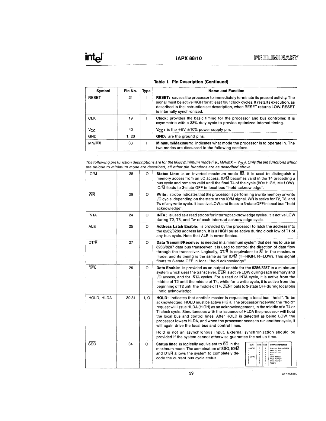
SSO | 34 | 0 | Status line: is logically equivalent to SO in th~ |
|
|
| maximum mode. The combination of SSO, 10/M |
|
|
| and DT/R allows the system to completely de- |
|
|
| code the current bus cycle status. |
-
101M | DTifi | §SO | CHARACTERISTICS |
:,"'0><) | 1! | : | Interrllpt Ac,nowledge |
| Read IIOporj | ||
| ~~::e 110 port | ||
| , |
|
|
,CodaaccaS$
,Read memory
,Wntememory
0Passive~ <,OWl
39 | AFN·QOB26D |