HARDWARE DESIGN
Conveniently, most. Intel peripherals, EPROMs and RAMs in the iAPX 88 family provide output enable or read inputs which prevent this from happening.
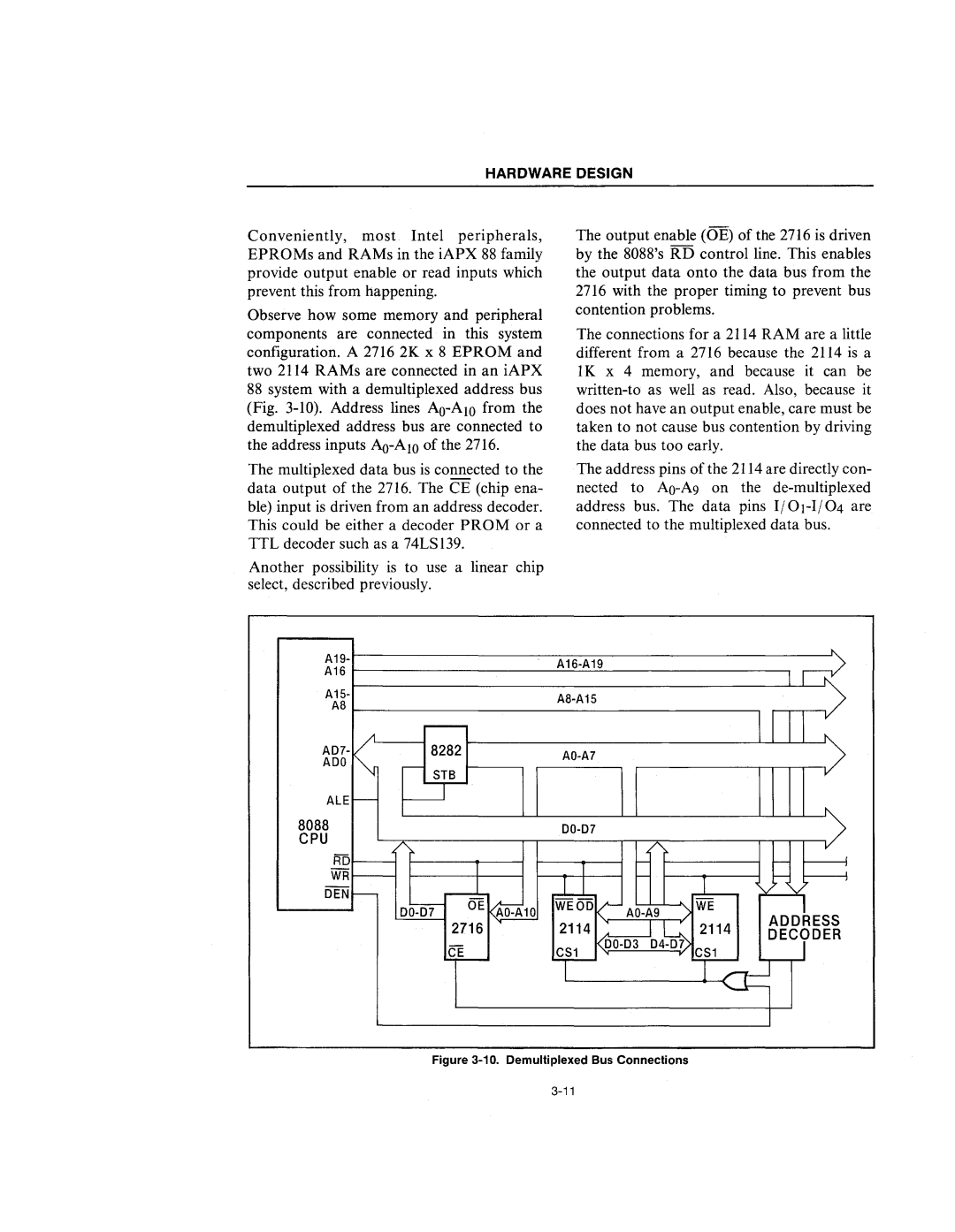
Observe how some memory and peripheral components are connected in this system configuration. A 2716 2K x 8 EPROM and two 2114 RAMs are connected in an iAPX 88 system with a demultiplexed address bus (Fig.
The multiplexed data bus is connected to the data output of the 2716. The CE (chip ena- ble) input is driven from an address decoder. This could be either a decoder PROM or a TIL decoder such as a 74LS139.
Another possibility is to use a linear chip select, described previously.
The output enable (OE) of the 2716 is driven by the 8088's RD control line. This enables the output data onto the data bus from the 2716 with the proper timing to prevent bus contention problems.
The connections for a 2114 RAM are a little different from a 2716 because the 2114 is a lK x 4 memory, and because it can be
.The address pins of the 2114 are directly con- nected to
A19- |
|
|
|
|
|
| ~ | |
A16 |
|
|
|
|
|
| ||
|
|
|
|
|
|
| ||
|
|
|
|
|
|
|
| |
A15- |
|
|
|
|
|
|
| |
AS |
|
|
|
|
|
|
| |
|
|
|
|
|
|
|
| |
| k: | ro - |
|
|
|
|
|
|
ADD | , - STB |
|
|
|
|
|
| |
AD7- |
| 8282 |
|
|
|
|
| |
ALE - | ~ |
|
|
|
|
|
| |
8088 |
|
|
|
|
|
|
| |
CPU |
|
|
|
|
|
|
|
|
RD - | r | T | r- |
|
| r- | ;==! | |
WR - | r- |
|
| I - | ||||
| - | ~Atui | ,llr |
| WE |
|
| |
DEN |
|
|
|
|
| I |
|
|
| 2716~ | 2114 |
|
| 2114 ADD~ESS | |||
|
| WEOD |
|
|
| |||
|
|
| T- | 04~ |
| DECyDER | ||
|
|
|
|
|
| |||
|
| CL- |
|
| CS1 |
|
| |
|
|
|
|
| l~ |
| ||
|
|
|
|
|
|
| ||
I