Page
MCS-48 Family of Single Chip Microcomputers Usersmanual
September
Credit
BXP
Multibus
Prompt
Table of Contents
Chapters
8051/8751/8031 Microcomputer
Insite UsersLibrary
Emulation Board
Emulation Board 10-19 UPP-103 Universal Prom Programmer
Packing Information
Page
Ntroduction
Page
Introduction to MCS-48
Introduction
5.0 and 10.0 J,Lsec Cycle Versions
8021 is code compatible but not pin compatible with
Introduction
Til
Eprom
Introduction
Architecture of a CPU
Function of a Computer
Typical Computer System
Accumulator
Program Counter Jumps, Subroutines and the Stack
Address Registers
Three levels of subroutines may be ac- commodated
Instruction Register and Decoder
Arithmetic/Logic Unit ALU
Timing
Control Circuitry
Computer Operations
Instruction Fetch
Memory Write
Input/Output
Interrupts
When finished the processor continues on
To the next instructions
Step Hex Code
Step No. Hex Code Assembly Code MOV RO, #32
Our machine language program then becomes
MOV R2, #05
ADD A, # ALFA*BETA/2
Cpla ADD A, REG
SUB R7
Education
Hardware Configuration
Developing An MCS-48 Based Product
Function Definition
Prompt
Intellec Development System
Production
Page
Single Component MCS-4S S~stem
Page
Summary
Architecture
Arithmetic Section
~BUS
Single Component System
Location
Single Component System
Input/Output
Single Component System
R23
Pointer
Jump Conditions
+--1 R
Interrupt Timing
Clock and Timing Circuits
As a Timer
As an Event Counter
Oscillator
ALE --f---+--+
111
Instruction
LOVI
Power Down Mode
BUS PCO·7
RUN Stop
Pin Description
Prog
00-07
Designation
Number Function
Reset
Programming, Verifying and Erasing Eprom
Single Component System
Single Step
Reset
Test and Debug
Disabling Internal Program Memory
Reading Internal Program Memory
Program Memory
Following is a functional description of the major elements
Timer/Event Counter
Oscillator and Clock
Input/Output Capabilities
QUASI-BIDIRECTIONAL Port Structure
1 T1 Input
High Current Outputs
Expanded I/O
10 CPU
Reset
Carry Flag Timer Overflow Flag
Jump Test Condition Instructions Accumulator
Functional Specifications
Program Memory
Data Memory
Port 0 Comparator Inputs
15Timer/Event Counter
Oscillator and Clock
See the 8021 description, .8, for a com- plete explanation
High Current Outputs
Expanded 1/0
Test and Interrupt Inputs
1-3 VAC
Ill
Analog to Digital Converter
19 CPU
Expanded
Page
Summary
Expansion of Program Memory
Expanded MCS-48 System
Interrupt Routines
AI? Latch
ROM
Latch
Expansion of Data Memory
IOW
Expansion of Input/Output
EXPAND!!D MCS-48 System
II AA
Read OO-Port #4 Write Port #5 10 or Port #6 Port #7
Keyboard
RD Display
Expanded MCS-48 System
Expansion Examples See Also Chapter
Multi-Chip MCS-48 Systems
Memory Bank Switching
=====ll 8~~5
BUS Port Operations
Control Signal Summary
Port Characteristics
Port 2 Operations
000
Page
Page
Instruction SET
Instruction SET
Subroutines
Instruction SET
Instruction SET Summary
8021
Instruction SET Summary
RET
Symbols and Abbreviations Used
DBF
PSW
Addc A,R r Add Carry and Register Contents to Accumulator
ADD A,R r Add Register Contents to Accumulator
ADD A,@R r Add Data Memory Contents to Accumulator
ADD A,#data Add Immediate Data to Accumulator
Addc A,#data Add Carry and Immediate Data to Accumulator
ANL A,R r Logical and Accumulator With Register Mask
ANL A,@R r Logical and Accumulator With Memory Mask
ANL A,#3+X/Y Andacc Contents with Value of EXP 3+X/Y
ANL A,#data Logical and Accumulator With Immediate Mask
Anld Pp,A Logical and Port 4-7 With Accumulator Mask
MOV RO,#50 Move 50DEC to Address
Andport 4 Contents
With ACC Bits
INC RO Increment REG RET Return to Main Program
11010 Flag 1 is cleared to zero F1-0
10010101111 Contents of the accumulator are cleared to zero
Cpla CPL Aacc Contents are COMPLE- Mented to
11 00 0 Flag 0 is cleared to zero
ADD SIX to Bits
DA Aacc Adjusted to 00000001 with C SET
AC 7 4 3 0 o 1 0 ADD SIX to Bits 010100001
Overflow to C
Example Decrement contents of external data memory location
DEC Rr Decrement Register Not in 8021
Ento ClK Enable Clock Output Not in 8021,8022
EN I Enable External Interrupt
EN Tcnti Enable Timer/Counter Interrupt Not
A,Pp Input Port or Data to Accumulator
INC a Increment Accumulator
INC Rr Increment Register
INC @R r Increment Data Memory Location
JBb address Jump If Accumulator Bit is Set Not in 8021
IputoPort 0 Data to Accumulator 8021, 8022 Only
INS A,BUS Strobed Iput of BUS Data to Accumulator
JC address Jump If Carry Is Set
Jmpp @A Indirect Jump Within
JF1 address Jump If Flag 1 Is Set Not in 8021
JMP address Direct Jump Within 2K Block
JNC address Jump If Carry Is Not Set
JNT1 address Jump If Test 1 Is Low
JNI address Jump If Interrupt Input is Low Not in 8021
Jnto address Jump If Test 0 Is Low Not
JNZ address Jump If Accumulator Is Not Zero
Jump to Location 53 DEC
Jump to Timerroutine
IFTF=1
Jump to Countroutine
MaV A,@R r Move Data Memory Contents to Accumulator
MaV A,PSW Move PSW Contents to Accumulator Not in 8021
MaV A,R r Move Register Contents to Accumulator
Mev A, #data Move Immediate Data to Accumulator
Mev A,T Move Timer/Counter Contents to Accumulator
MaV @Rr,A Move Accumulator Contents to Data Memory
Movo A,Pp Move Port 4-7 Data to Accumulator
Movo Pp,A Move Accumulator Data to Port
Movp A,@A Move Current Page Data to Accumulator
Not in 8021
Maxdm Movx A,@R1 Move Contents of Location
MOVP3 A,@A Move Page 3 Data to Accumulator Not in 8021,8022
Current page are Moved to ACC
ORL A,@Rr Logical or Accumulator With Memory Mask
NOP The NOP Instruction
ORL A,Rr Logical or Accumulator With Register Mask
ORL A,#data Logical OFJ Accumulator With Immediate Mask
8021
Outl Pp,A Output Accumulator Data to Port 1 or
Retr Return With PSW Restore Not in 8021
Rrtc RRC a Carry is SET and ACC
Rrnc RR Anew ACC Contents are
Example Assume carry is not set and accumulator contains
Contains
Jump to Location
SEL MBO Select Memory Bank
JMP $+20
48 HEX
Jump to Routine Intif ACe
Stop Tcnt Stop Timer/Event-Counter
10110101011
BIT 3 is SET REG 7=8
Strt T Start Timer
Strt CNT Start Event Counter
Swap a Swap Nibbles Within Accumulator
XCH A,R r Exchange Accumulator-Register Contents
XCH A,@R r Exchange Accumulator and Data Memory Contents
Xchd A,@R r Exchange Accumulator and Data Memory 4-Bit Data
XRL A,@Rr Logical XOR Accumulator With Memory Mask
XRL A,@R1 Xoracc Contents with Mask Location
XRL A,Rr Logical XOR Accumulator With Register Mask
XRL A,#data Logical XOR Accumulator With Immediate Mask
Appli~ation Examples
Page
Introduction
Crystal Oscillator Mode
LC Oscillator Mode
Driving from External Source
Reset
Application Examples
~~J
Rvv-i T1
Multiple Interrupt Sources
Tf ~r
Ii6
Serves as address latch
Tt-2 A7
17&A3
Xtali
ROM
=!-39TO
Both 1/0 and RAM are addressed as data memory
This configuration is explained in section
Reset
F1L
Expander
~fd...L
Pinnumbers are Different for
~1~
DB6 r
Adding 8 Input Lines
Application Examples
·15
Adding Output for KEYBOARD/DISPLAY Scanning
JfL
RT T T T T
Application Examples Emulator Circuit DESCRIPTION-6 MHZ
Substitute a
Interface to Drum Printer
Timer
RAM
II Keyboard Display
Microwave Oven Controller
Double Load
Double ADD
Double Subtract
Double Store
Double Right Logical Shift
Application Examples Double Exchange
Double Left Logical Shift
Double Right Arithmetic Shift
Application Examples Binary Multiply
Interrupt Handling
CPL Subtract Second from First INC
Application Examples Byte Processing System
R1,A
2sCOMPLEMENT and ADD
8 MULTIPLY-ASSEMBLED by MCS-48 Macro Assembler
See AP-49
IIn ·1
APP\,JCATION Examples
16 x 8 DIVIDE-ASSEMBLED by MCS-48 Macro ASS.E.MBLERSEE AP-49
16 x 8 DIVIDE-ASSEMBLED by MCS-48 Macro Assembler see AP-49
Page
MCS-4STMComponent
Page
Hmos Single Component 8-BIT Microcomputer
IIH!T
Signal occurs once during
Used to enable data onto
Address latch enable. This
Program store enable. This
S04SH/S04SH-1 /S035HL-1/S035H L-1
Inter 8048H/8048H-1/8035HL/8035HL.1
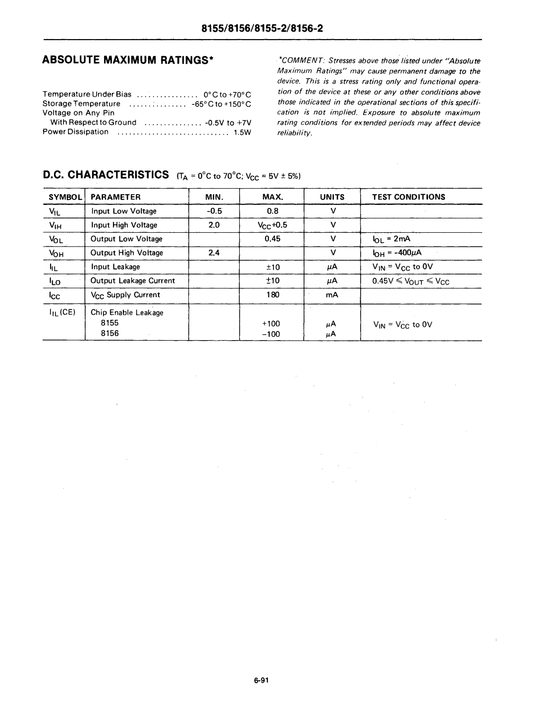
Absolute Maximum RATINGS·
Port 2 Timing
BUS Timing AS a Function of TCY
Read From External Data Memory
S04SH/S04SH-1/S035HL/S035HL-1
Waveforms
8035HL
8048H/8048H·1/8035HL/8035HL·1
J3 Xtal Z
PIN Configuration Logic Symbol Block Diagram
Rll
PIN Configuration Logic Symbol
Block Diagram
8048/8035L/8748/8748-6/8748-8/8035/8035-8
PIN Description
AFN-Q1354A-03
VOL =2.0 mA
All Except XTAL1, XTAL2, Reset
Input High Voltage X1, X2, RESEi
Output Low Voltage 10L = 1.8 mA
===i---h·1
Characteristics Port 2 Timing
Driving from External Source
Crystal Oscillator Mode
LC Oscillator Mode
PROGRAMMING, VERIFYING, and Erasing the 8748 Eprom
TA = 2SOC ± SoC, Vee =SV ± S%, Voo = 2SV ±
Waveforms for Programming
Verify .I.~---PROGRAM
PROMPT-48 Microcomputer Design Aid, or
Intel Corporation
108048/8748/8035L
108048/8748/8035L
Absolute Maximum RATINGS·
Operating Characteristics
IDS0481S7481S035L
BUSP1, P2BUS, P1, P2
TOR Data Hold
TAW Address Setup to WR
260 TAD Address Setup to Data
PSEN, RD to Data
TpL Port 2 I/O Data Setup
Characteristics
Top Port Control Setup Before Failing Edge of Prog
TA= -40·Cto +85·C, Vcc=5V ±10%, Vss=OV
+-----t XTALl
Crystal Oscillator Mode Driving from External Source
Reset
Prog
TA =25C ± 5C, Vee =5V ± 5%, Vee =25V ±
TA = 25C ± 5C, Vee = 5V ± 5%, Vee = 25V ±
Waveforms for Programming
PROMPT-48 Microcomputer Design Aid. or
Inter
Lcoscillator Mode
Voo
Programming Verification
Voo Program Voltage High Level 24.0 2S.0
IPH
Unit Test Conditions
EA Program or Verify Voltage High Level 21.5 24.5 8748
EA 5
M8048/M8748/M8035L
M8048/M8748/M8035L
Pin #
Prog
Tpo Output Data Hold Time Tpp Prog Pulae Width
Tcp Port Control Setup Before Falling
TpL Port 2 1/0 Data Setup
TLP Port 2 1/0 Data Hold 120
Characteristics
ALE JI ~----r---I L
AN D Operati NG Characteristics
BUS, P1, P2
Inter
80411803118031
8049/8039
Operating Characteristics
Symbol Parameter Min Max Unit
ALE JIL --------..1.--1----L
18049/8039
Mask Programmable ROM External ROM or Eprom MHz Operation
INr
IntJ18049/8039
Til
VOL2
VIH1
BUS, RD, WR, PSEN, ALE
BUS, RD, WR, PSEN, ALE VOH1
TAFC--1 I~OATING-I t=t or
Waveforms
TA = -400C to +850 C, Vee = Voo = +5V ±10%, Vss = OV
Output Data Setup Time 230
Port 2 1/0 Data Setup 300
Unit Conditions Note
Crystal Oscillator Mode LC Oscillator Mode
XT AL1
PIN Configuration Logic Symbol Block Diagram
8021
VIH10% Input high voltage all except Xtal 1
OC to 70C
V1Hl Input High Voltage Xtal 1 & 2, T1
T1, RESEl
ALE
XTAL2
8022
VTH
Reset Avss
Prog POO-P07
Varef ANO,AN1 ALE Xtal
8022
Fzx
IpAL---ooj·1
Port 2 Timing
AID Converter Characteristics
Analog Input Timing
Analog Input 0, Analog Input Timer
Mnemonic for in-page Operation
CNT
Inter
PIN Description
GND
Absolute Maximum Ratings
~~x
125
P20-P23 -- .....--X..... ...Jr
108243
14P52
18243
GND
18243
Tes
# pins= 60 mA-+- 8 mA/pin = 7.5=
1 2 3 4 5 6 7 8 9 10 11 12
Output Expander Timing
16,384·8IT ROM with
CE2
Reset
CE1
Ready
III
Symbol Parameter MIN MAX
8355/8355-2
ILO
+- Al ~
Cl ~
Input Mode
Output Mode
8355/8355·2
PIN Configuration Block Diagram
Directly Compatible with SOS5A CPU
8755A
8755AFUNCTIONAL PIN Definition
PROG/CE1
UPPI41
SA Programming Module Cross Reference Module Name USE with
UPP
UPP UP2121
Comment
Symbol Parameter MIN MAX VIL
8755A
Ready Hold Time
Clock Specification for 8755A
Prom Read, 1/0 Read and Write Timing
Wait State Timing Ready =0
Specification Programming
ITA =OC to 70C Vee =5V ± 5% Vss =OV
Voo Programming Voltage during Write To Eprom
Program Mode Timing Diagram
8155-2
Enable
8085A 8085A-2
8156-2
Timer OUT
8155/8156/8155-2/8156-2
8155/8156 PIN Functions
Description
8156 Internal Registers
Programming Command Register
Reading the Status Register
BFLowLow INTRLowHigh
Control Input Mode Output Mode
INPUT/OUTPUT Section
STB
8155/8156/8155-2/8156-2
Pca
Timer Section
Example Program
8085A Minimum System Configuration
Interval Timer Interrupt Levels
WR AD ALE
Symbol Parameter MIN MAX Units Test Conditions VIL
Symbol Parameter
MIN MAX Units
Read Cycle
Write Cycle
8155/8156/8155-2/8156-2
WI\ J / j
Basic Input Mode
Basic Output Mode
PIN Configuration Block Diagram
PIN Names
Operational Description
Truth Table for Power Down and Function Enable
8185/8185-2
Truth Table for Control and Data BUS PIN Status
Absolute Maximum Ratings
Comment
8185/8185-2
Page
Page
SINGLE-COMPONENT 8-BIT Microcomputer
MACRO-VIEW of the 8051 Architecture
0INTRODUCTION
8051 Family
8051 CPU Architecture
ON-CHIP Peripheral Functions
1Interrupt System
21/0 Facilities
8031/8051/8751
3Timer/Event Counters
8031/8051/8751
8031/8051/8751
4Serial Communications
~=- J~~====~
~DATA
8031/8051/8751
Circuit ground potential
XTAL2
Psen
XTAL1
Family Development System and Software Support
Workshop
Symbol Parameter Min Typ Max Units
Universal Prom Programmer Personality Card UPP-851
Insite Library
12MHz Clock
Data Memory Write Cycle
Inter8031/8051/8751
8051 Instruction SET Summary
Inter
All mnemonics copyrlghted@ Intel Corporation
Page
Compatible MCS-48 Components
PIN Configuration
1024 X 4 BIT Static RAM
2114A Family
Symbol Parameter
Address -..II-------------i--l
Unit
Typical D.C. and .A.C. Characteristics
Normauzed Access Time VS Supply Voltage
2316E 16K 2K 8 ROM
2316E
Data ----=HIGHZ~--~~~~~~~~~~-OU-T~TV-ALIO~~~JlJJI
PIN Configuration
PIN Connection During Read or Program
Family
BB Power Supply 5V±5% 5Vt.5% -5V±5% -5V±10%
Operating Characteristics
Nco and A.C.OPERATING Conditions During Read
Input Capacitance
Address to Output Delay
2708·1 limits 2708·6Limits Units
VIN = OV
Family
Waveforms
PIN Configuration Mode Selection
PIN Names
Programming
CE = VIH. OE = VIL
2716
Cout
2716
Typical 16K Eprom System
2716
Device Operation
Two Line Control
Approved
8086·2 MPU .. .Zero Wait State
Industry Standard Pinout . .. Jedec
8205
Ei==~ fEH2·E3
Applications
A13 --..,-H+-q E
8205
Eii-+-IH-+t-t r
State Decoder Circuit
TA = O·Cto + 75·C, Vee = 5V ± 5%
Typical Characteristics
\.. ~ ~
MIN MAX
Conditions of Test Test Load
Switching Characteristics
Charactristics
Test Waveforms
GD ~s ------- + H
PIN Configuration Logic Diagram
IT os
DB ---------- -- +i
+-+1
Functional Description
Il D
IE D
Gated Buffer
Basic Schematic Symbols
II. Gated Butter 3-State
DS2 , ------,----.J
8212
Here the 8212 is used as the status latch for an 8080A
VI. Output Port With Hand-Shaking
~DI, Stbdo LOW Order
AD2
Bossa AD4 AD5 AD6 AD7
CLR
Input Load Current, ACK, OS2, CR VF = A5V
8212
Output Currents 100mA
IOL = 15mA
Ffi
Ili
052. CK. ACK. DI1-Dls Input Capacitance 5pF
Switching Characteristics
Typ. Max CIN 051 MD Input Capacitance 9pF 12pF
DOs Output Capacitance 8pF
TCI
II,D
SGS
821413214
Icex
8214/3214
Capacitances
Inte
Test Conditions Test Load Circuit
·BITPARALLEL Bidirectional BUS Driver
001
Bidirectional Driver
Control aatlng OlEN, CS
Waveforms Characteristics
OUT O---T
IFI IF2 IRI IR2 VIL VIH
Voli VOL2
821618226
Applications of the 8216/8226
010
8282/8283
Octal Latch
VCC
PIN Definitions Operational Description
PinD.scrlptlon
Tshov
VOL VOH
Tivov
Tehoz
JJ\~ J/~~
8282/8283
Intel
Vee
Ao-A7
Bo- B7
Characteristics for 8286/8287
Output Delay vs. Capacitance
Jk~
Output
Page
Page
Synchronous and Asynchronous Operation
Synchronous 5·8 Bit Characters
Features and Enhancements
Capacitance
Capacitance pF
Iofl
Bus Parameters !Note
Input Waveforms for AC Tests
MIN MAX Unit
Programmable Interval Timer
General
VIIi -.,--.,q
System Interface
Control Word Register
Programming
Operational Description
General
Control Word Format
825318253·5
Mode 2 Rate Generator
=41 I---t--n --+
8253/8253-5
LSB
MSB
Read Operations
Read Operation Chart
Mode Register for Latching Count
Reading While Counting
Oe to 700 e
Re.dCycle
Bus Parameters Note
Input Waveforms for A.C. Tests
Write Timing
825318253·5
Clock and Gate Timing
PIN Configuration 8255A Block Diagram
Programmable Peripheral Interface
8255A Basic Operation
8255A18255A·5
8255A Functional Description
Face peripheral devices or structures
Group a and Group B Controls
PIN Configuration PIN Names
8255A18255A·5
Ports A, B, and C
Mode Selection
Single Bit Set/Reset Feature
8255A Operational Description
Operating Modes
Interrupt Control Functions
Mode 0 Port Definition
Mode 0 Configurations
8255AJ8255A·5
PA7·pAo
II I I I, I0 I0 I0
IBF Input Buffer Full F/F
Input Control Signal Definition
TPH
Intr Interrupt Request
Intea
Output Control Signal Definition
10 I ·IOMXlXl
Inte B
Output Operations
Combinations of Mode
Bidirectional Bus 1/0 Control Signal Definition
Input Operations
8255.Al8255A·5
LtAOi
ErXtJ I 0\
\, I, erXtJ I0\
Mode Definition Summary
30AFN-00744A-14
Only
Applications of the 8255A
Printer Interface
PC, r
MSB
Capacitance
Read
MIN. MAX Unit
CIR
TwB
TRIT LtR1Bj
SIB-Ii
Programmable Interrupt Controller
SP/EN
8259A
Interrupts in Microcomputer Systems
8259A Basic Functional Description
Interrupt Mask Register IMR
Interrupt Request Register IRR and IN·SERVICE Register ISR
Priority Resolver
INT Interrupt
Cascade BUFFER/COMPARATOR
8259A
8259A Interface to Standard System Bus
Interrupt Sequence
~O ~ ~
General
Disable Function
Programming the 8259A
Input Operation Read
Initialization Command Words 1 and 2 ICW1,ICW2
Initialization Command Word 3 ICW3
0 I 0 I 0 I 0 I 0 lID, liD, lIDo
8259A
Operation Control Word 2 OCW2 Operation Control Words Ocwi
Operation Command Words OCWs
Operation Control Word 1 OCW1
Ocwa
Operation Command Word Format
OJNTl
R,-r-- I-i-Ioo r,-r,-r
Fully Nested Mode
Special Mask Mode
Buffered Mode
Special Fully Nested Mode
Rotating Priority Mode B Rotation by Software
Word enabled onto the data bus during m5 is
Automatic END of Interrupt Aeoi Mode
Wol
This mode is programmed using bit 3 in ICW1
Priority Cell Simplified Logic Diagram
Level Triggered Mode
OH-++-+
8272
Registers CPU Interface
Features
8272
Description
8272
Polling Feature
Reset to the Interrupt signal
IntJ
Command SET
Command Descriptions
Read Data
Write Data
Transfer Capacity EN End of Cylinder Flag No No Data Flag
Read a Track
Write Deleted Data
Read Deleted Data
Readid
Scan Commands
Specify
Recalibrate
Sense Interrupt Status
Sense Drive Status
Status Registers BIT Name Symbol Description
Usa
CINI»
DC Characteristics
VIL CLK & WR CLK VIH
VIN=OV
ICY
~-----~---V
Sel-I
Timing Measurement Conditions
LI3
Block Oiagram
8273, 8273·4, 8273·8
Brief Description of HDLC/SDLC Protocols
32XCLi
Flag DET
Programmable KEYBOARD/DISPLAY Interface
RAM
827918279-5
Hardware Description
Principles of Operation
827918279·5
Software Operation
Data Read
End Interrupt/Error Mode Set
Status Word
Data Write
Interface Considerations
Scanned Keyboard Mode, 2·Key Lockout
===~
General Block Diagram
Applications
Symbol Test TYP MAX
VIL2
IIL1
Input Waveforms for A.C. Tests
BUS Parameters
8279
Scan Timing Scan Waveforms
Display Waveforms
Gpib TALKER/LISTENER
8291
General Purpose Interface BUS Gpib
System Diagram
8291
General Description
Acrs
Acds
Pacs
Ppas
Remote Messages Received ATN SH,AH,T,TE,L,LE,PP,C DAB
SH,AH,T,TE,L,LE,SR,RL,PP,C
AH,C
DAC
DAV
Remote Messages Sent ATN DAB
DAC
END
All Write Registers
DontCare
SPAS---SPAS Spasc Llcno LLO Lloc
Interrupt Registers
Menting this feature, with 80 and Bi enabied from
ITO ILO I 0 I 0 I 0 I 0 Admi Aomoi
Command Pass Through Register
Provided for
Section on Parallel Poll Protocol
Auxiliary Mode Register
Auxiliary Commands
Auxiliary Register a
Internal Counter
2NF
Auxiliary Register B
Reset Procedure
Parallel Poll Protocol
8291 Using DMA 8291 to 8291A Software Compatibility
Ilol
Device Electrical Characteristics
VOH-INT
Iloh
TwA~
Timing Waveforms
Gpib Timingsii
Modified State Diagrams
Figure A.1 State Diagrams next
101
Settling Time for Multiline Messages 21st
Response to ATN 200ns Interface Message Accept Time t
TE,L,LE,C,CE
Figure C-l -Wire Handshake Timing at
Appendix C
Figure C.2. Handshake Flowchart
IIIL---,--11 ,--I
105
Gpib Controller
106
Ai1W
Gpib Transceiver
BUS9
EOI
BUS1
OATA1
Gpib
Mode 0 PIN Description
=OV
NDAC* I/O
Nrfo
TIL
Ieee Gpib
Mode 1 PIN Description
Mode 2 PIN Description
Ndac
Nrfd
Ieee
Mode 3 PIN Description
R1L
LIEN
TiR1
Absolute Maximum Ratings
Operating Characteristics
8293
Capacitance
TYP.· MAX
Characteristics
TA = O·Cto 70·C Vee= 5.0V ± 10% GND = OV
·118
Output Loading Test Circuits
8293
Waveforms
8294
8295
·122
====J
123
UPI·41A Features Enhancements
Signal Description
Mnemonic Description Bytes Cycles
Data Moves
8041 Al8641 Al8741 a
VIU
IU1
Read OPERATION-DATA BUS Buffer Register
Input and Output Waveforms for A.C. Tests
Typical 8041/8741A Current
Write OPERATION-DATA BUS Buffer Register
CHARACTERISTICS-PORT
CHARACTERISTICS-DMA
WAVEFORMS-DMA
PROGRAMMING, VERIFYING, and Erasing the 8741A Eprom
VOO
Timing Specification for Programming
Specification for Programming
Vdol
Program
8041Al8641 Al8741A
Support Products
Page
Microcomputer Development System
Credit
MODEL225 Functional Description
10-2
Peripheral Interface
InterMODEL225 System Components
Integral CRT
Control
Specifications
9800556
Notavailable on bus
110V, 60 Hz 5.9 Amp 220V, 50 Hz 3.0 Amp
9800292
Page
Intellec Prompt MCS·48 Microcomputer Design AID
Intellec Prompt Features
Single Component Compu.ter
Prompt 48 Commands and Functions
Intellec Prompt
Intellec Prompt Functional Description
MCS-48 Processors
User Interrupt causes an Interrupt only If
Prompt system Is running a user program
Cycle Time tCY = 2.5,..s Clock 6 MHz ± 0.1%
Ordering Information
MCS·48 IN·CIRCUIT Emulator
~ L ·
ICE·49
Memory Mapping
GO from .START Till XDATA. Rslt Written
ICE·49
ISIS·II
EM1 Emulation Board
EM1
Ordering Information
EM1 Specifications
DC Power Vcc5V ±5% Icc 300 mA max
MDS·EM1
EM2 Emulation Board
ANO
40·PIN Socket Configuration EM2 Block Diagram
EM2
AN1
EM2
UPP-1P3
MDS-EM2
Canadian Sales Offices
September
Canadian Distributors
TAvnet Electronics McCormick Avenue Costa Mesa
IntJ
Bowers Avenue International Sales and Marketing Offices
International DISTRIBUTORS/REPRESENTATIVES
International Sales and Marketing Offices
INTEL$ Marketing Offices
Canadian Service Offices