This document supports firmware version 2.2 and above
Page
Warranty
How to Reach Customer Service
TEK-WIDE
Table of Contents
Tutorial
Table of Contents
Menus
Gpib
Theory of Operation Glossary Glossary-1 Index Index-1
List of Figures
List of Tables
Safety
Do Not Remove Instrument Covers
SMA Connectors
Behavior of Outputs Turning Power On or Off
Static Sensitive Device Notice
How This Manual is Organized
Conventions
Related Manuals
Xvi
Getting Started
GB1400 Pattern Generator and Error Detector
Features
Prbs Or User-Defined Test Patterns
Symmetrical, Low-Jitter Output Waveforms
Applications
Sample Applications
Powerful Analysis And Reporting Functions
Adjustable Inputs For Maximum Flexibility
Auto Search For Easy Setup
Burst Mode
GB1400T
Ordering Information
GigaBERT GB1400
GB1400R
GB Comparison GB660/CSA907A GB700 GB1400 Feature Tx and Rx
GB1400 Instrument Configurations Standard and Burst Option
GB1400 with Burst Option
Initial Self-Check Procedure
Procedure
Page
Operating Basics
Functional Overview
Bert Basics GB1400
Example, Bert Application
Clock Data
Controls, Indicators and Connectors
Front Panel, GB1400 Generator Tx
Front Panel, GB1400 Analyzer RX
Generator Tx Display
Display Formats
1405000 PN23
Frequency kHz Pattern Output
1405000 0E-06 2410538 PN23
Frequency kHz Error Rate Totalize
Delay/ Memory
Analyzer RX Display
Page
Outputs and Inputs
Generator Output Connectors Section
= clock bar = not clock
Generator Clock Section
Generator Output Section
Generator Rear Panel
Changing the Line Fuse
Analyzer Input Section
Analyzer Monitor Section
Analyzer Rear Panel
Connectors, Terminations, and Levels
DATA/DATA BAR
Reset to Factory Default
Controls and Indicators
Power Switches
View Angle and Panel Lock Keys
Gpib Section Controls
Pattern Controls and Function Keys
Function Soft Keys F1, F2, F3, and F4
Analyzer Inputs
Generator Error Inject Section
Affected Input Allowable Control
Analyzer Error History Section
Sync Loss
Analyzer Error Detection Section
Analyzer Sync Controls
Burst Mode Option
Burst Mode Usage
Specifications for Burst Mode
Transmitter Burst Mode Option
Data Value
Pecl Option for GB1400 Tx
Display Setting
ECL Levels Pecl Levels
Objective of Tutorial
Basic Bert testing with the GB1400
Key Feature of Tutorial
Equipment Required
Setup units with default settings
Instrument Connections and Controls
Setup Generator for PRBS-23 Mode
Connect the Generator to the Analyzer
Setup Analyzer for AUTO-SEARCH Operation
Change the Prbs pattern type
Turn off Auto Search and change Generator Outputs
Key several times to setup the analyzer for totalize
Error Rate display shows no Data or a 50% Error Rate
Data signal not detected. Selected
Your data signal
You are starting to detect the data signal
This Concludes the Tutorial
Applications
Two Auto Search Synchronization Methods
Phase
Application Note Auto Search Synchronization
Auto Search Algorithm Fast Method
Auto Search will find the Data Delay
Auto Search will find the Data V-THRESHOLD voltage
Auto Search will find the Data Pattern and Polarity
II. Auto Search Algorithm BER Method
Auto Search will then attempt to find the Data Pattern
Auto Search will determine the Data Delay
Page
Consideration In Determining The Eye Data Width
Delay Specifications
Consideration In Determining The Data Eye Center
GB700/ GB1400 Optical Component Test
Fiber Optic Link Test Example
Fibre Channel Link Testing Parallel and High-speed Serial
Testing Qpsk Modems, I & Q
Qpsk
Qpsk BER Testing using Prbs Data for 2-Channel I & Q
Channel Bert
Application Example
Reference
Functions Common to Generator TX and Analyzer RX
Turning Instrument Power ON/OFF
Menu Overview
Selecting 115 VAC or 230 VAC Operation
Locking the Front Panel
Recalling the Default Setup
Selecting a Pattern
Pattern Definitions
Selecting the Current Word Pattern
Selecting the Active Pattern
Selecting Prbs Patterns
Prbs 2n-1 Test Patterns
Selecting RECALLing a Saved Word Pattern
Word
Basics
Creating Word Patterns Using Front Panel Controls
Word Patterns
Standard Instruments
Instruments Equipped with 1-Mbit Option
Length Fill
Creating Word Patterns Using Menus
Order
Creating Word Patterns Under Remote Control
Saving Word Patterns 1-Mbit Memory Option
Recalling Word Patterns 1-Mbit Memory Option
External Clock Input
Generator TX Functions
Clock Source and Frequency
Clock Source
Saving a Frequency
Recalling a Frequency
Data and Clock Outputs
Overview
Generator Clock and Data Output Equivalent Circuits
Output Setup Rules vs. Termination Impedance
Amplitude and Baseline Offset
Logically Inverting Output Data D-INV
Single-ended or Differential Operation
Procedure for Single-ended Operation TX only
Procedure for Differential Operation TX only
Pattern Sync and CLOCK/4 Outputs
Error Injection
Selecting an Error Inject Mode
Procedure to Control Error Injection Mode
Error Inject Input
Data Inhibit Logic
Analyzer RX Functions
Automatic Setup Functions Sync
Disable Key
Auto Search Key
Actions Taken by Analyzer when Synchronization is Lost
Auto Search With Prbs Patterns
Relationship between Auto Search and Disable
How to Disable Automatic Pattern Resynchronization
Auto Search with Non-PRBS Patterns
Synchronization Lock Threshold
Procedure to Set Sync Threshold
Synchronization Threshold
Clock, Data, and Reference Data Inputs
Input Parameters
Procedure to Add Delay
Input Data Delay
How F2 and F3 Determine Which Input Can be Set Up
Controls
Input Termination
Procedure for Selecting Input Termination
Input Terminations for CLOCK, DATA, and REF Data
Logically Inverting Input Data
Input Decision Threshold
Input Threshold Range as a Function of Termination
Procedure for Selecting the Reference Data Mode
Selecting the Reference Data Mode
Singled-ended or Differential Operation
Output Setup
Monitor Outputs
Error Detection Set Up
BER
How Totalize Results are Measured
How Window Results Are Measured
How Test Results Are Measured
Window Measurement Process
Test Measurement Process
Procedure to Select a Results Display Mode
Display Mode Totalize, Window, or Test
Totalize Process Set Up
How to Tell Which Display Mode is Active
Window Process Set Up
Procedure
Test Process Set Up
Viewing Results
BER and Bit Errors
Procedure to View Desired BER and Bit Error Results
All Other Results Test Process only
Basic Report Setup Procedure
Printing Results Reports
Analyzer Setup Report
Example Analyzer Setup Report
End-of-Test Reports
Procedure to Enable or Disable End-of-Test Reports
Example End-of-Test Report
End-of-Window Reports
Procedure to Enable or Disable End-of-Window Reports
Example End-of-Window Report
Procedure to Enable On-Error Reports
On-Error Reports
Example On-Error Report
Procedure to Generate an On-Demand Test Summary Report
BER = TE / TB
Result Definitions
All Other Results Test Intervals Only
ES = TSE US
Located in the Error History section of the front
Error History Indicators
Analyzer performance history indicators are
Panel. These indicators will latch on when the indicated
Clear Control
Analyzer Error Messages
Procedure To Set Up the Audio Alert Function
Audio Beeper Function
Procedure for Stopping the Test Process
Procedure for Starting the Test Measurement Process
Starting and Stopping Measurements
Starting New Totalize and Window Measurement Intervals
Menus
Functions Performed Using the Menu System
Example Procedure Illustrating Menus and Functions
Menu and Function Pages
More Length Mode Report F1ESC F4SET Test Mode = Untimed
F1ESC F4SET Reports on = EOT/ERROR
General Rules for Using the Menu System
Menu Summaries
10. Menu Descriptions
11. Analyzer Menu System Overview
12. Generator Menu System Overview
Word
Menu Function Definitions
Word Edit Edit
F1ESC F2- -F3 F4SET
Word AT ddddd = bbbbbbbb
Format
Word Length Length
F1ESC F2- -F3 F4SET LENmmmmm Bytes + n Bits
Word Length
Fill Word Memory WITHhh
Word Fill Fill
Word Order Order
F1ESC F4SET Word Order = ccc First
Word Order
Word Synchronization Threshold Sync
Word Sync Thres LEVEL= d
Word Sync
Buffer
Buffer
Auto
Fast BER
Test Length Length
F1ESC F2- -F3 F4SET Test Length = hhmmss
Test Length
Test Mode Mode
F1ESC F4SET Test Mode = ccccccc
Test Mode
Test Reports Report
F1ESC F4SET Reports on = ccccccccc
Test Report
Test Threshold Thres
F1ESC F4SET Error Threshold = eeeee
Test Thres
Test Squelch Squel
On Error Squelch = ccc
Test Squel
Test Print Print
Test Print
Test View Previous VIEW-PRE
F1ESC F4SET result namecount %
Test VIEW-PRE
Test View Current VIEW-CUR
Test VIEW-CUR
Window Mode Mode
F1ESC F4SET Window Mode = ccccccc
Window Mode
Window Interval in Bits Bits
Format
F1ESC F4SET Window LEN = 1.0eEE Bits
Window Bits
Window Interval in HrsMinSec Second
F1ESC F2- -F3 F4SET Window LEN = hhmmss
Window Second
Window Reports Report
END of Window Print = ccc
Window Report
RS-232 Baud Rate Baud
Baud = dddd
Baud
RS-232 Parity Parity
F1ESC F4SET Parity = cccc
Parity
RS-232 Data Bits Size
Size = d
Size
RS-232 End-of-Line Char. EOL
F1ESC F4SET EOL = ccccc
EOL
RS-232 Xon/Xoff XON/XOFF
F1ESC F4SET XON/XOFF Enable = ccc
XON/XOFF
RS-232 Echo Echo
F1ESC F4SET RS232 Echo Enable = ccc
Echo
F1ESC F4SET Terminator = cccccc
Utility Option Option
Util Option
Utility Version VER
Util VER
Time Option Date
F1ESC F2- -F3 F4SET Date = mmm dd yy
Date
Time Option Time
F1ESC F2- -F3 F4SET Time = hhmmss
Time
Reference
Appendices
External Clock Source
GB1400 Generator TX
Internal Clock Source
SMA
Data Patterns
Data Output True and Complement
Clock Output True and Complement
Rear Panel Auxiliary Outputs Phase A, Phase B, Clock/2
Error Injection
NRZ-L
RS-232 and Gpib Interfaces
AC-Power Requirements
Mechanical
Clock Input
GB1400 Analyzer
Data Input
Reference Data Input
AUX
Synchronization
Measurements
BER
Printer Interface
Specifications
Bert Primer/ Technical Articles
Bert used to test physical layer
Bert Definition
Bert Building Blocks
Bert Pattern Generation
Prbs Patterns
Prbs
Prbs Generation Circuits a few sample diagrams
Doutput
Other Tx Patterns
Output Amplifiers
Bert Receiver or Error Analyzer Components
Bert Clock
Data Coding, NRZ
Data Input Amplifiers
Error Comparator
Received Data Pattern Reference
BER Computation
Confidence Level in BER Measurement
Confidence Requires Collecting Many Errors
Stress Testing
Additional Reading
Eye Width Measurement
Other Bert Features
Auto-Synch
Pattern Lock
Error Insertion
Pattern Loading Software
Jitter Generation
Bit error rate testing
How long is long enough?
BER
Ideal pulse
Stressing through pattern generation
Bert Technical Articles
Bert Technical Articles
Bert Technical Articles
Ensure Accuracy Of Bit-Error Rate Tests
Page
Supplying Data Patterns
Bert
Noise-Margin Stressing
Μ F Avergage = Average =
Page
Data patterns for clock recovery stressing
Data Patterns Stored
+ Peak
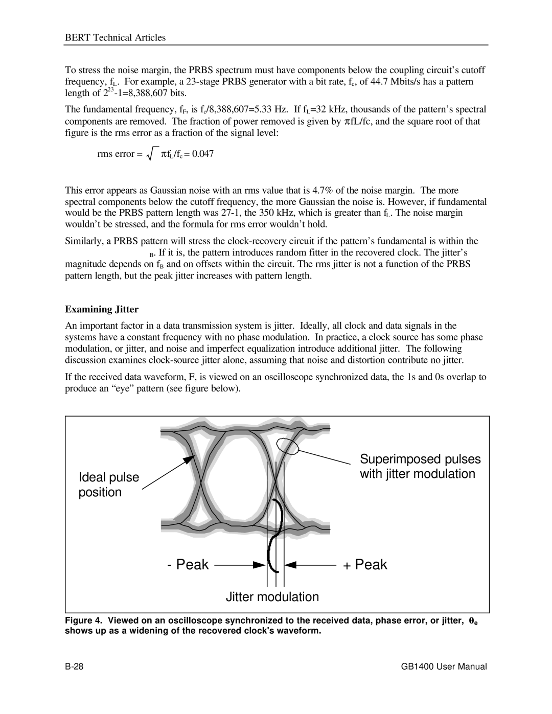
Examining Jitter
2f BΦ θif B
Amplitude UI peak-to-peak Frequency
Jitter Tolerance
Bert Affects Accuracy
Example of Error Rate Measurement
Abstract
BER Measurement Inaccuracy versus Test Time
= n / T
Inaccuracy 95% = 2 σ / n ≈ 2/ n
Testing for an Upper Limit on Error Rate
Reduced Test Time by Stressing
SNR = 20 log S / N rms
Attenuation dB
Example
BER
Example
BER
Summary
Poisson Error Process
Pn = rT n e−rT . n
BER
Biography
Remote Commands
Type of Commands Starts on
Overview
Datathres
DATATHRES?
Command Line Rules
Command Line Terminator
Setting Arguments Outside of Legal Ranges
Command Examples
Command Summary Alphabetical
Bytesync n Analyzer only Bytesync?
Remote Commands
Rescurrate?
Tse?
Cls
Ese n
Esr?
Ese?
Idn?
Opc
Lrn?
Opc?
Rst
Sre n
Sre?
Stb?
Tse v Analyzer Only
Tst?
Wai
Tse? Analyzer Only
Tsr? Analyzer Only
Datainvert?
Datainvert onoff
Datapattern prbs word rdata
Prbslength
Datapattern?
Prbslength?
Saveword m
Recallword m
Wordbits l, b1 b2
Wordlength l
Wordbits?
Wordmemlen m, l
Wordmemord?
Wordmemord m, msb lsb
Wordmemord? m
Wordmemory m, l, b1, b2
Wordmemory? m
Wordorder msb lsb
Example Wordorder lsb
Page
Wordorder?
Memory allocation for Word Memory storage
Wordmemory?
Gpibaddress?
Gpibaddress
Gpibbus offbus talklisten
Rsecho?
Gpibbus?
Rsecho onoff
Rspmtlf onoff
Rsxonxoff onoff
Rspmtlf?
Rsprompt s
Rspmtlf on
Rsxonxoff?
Allmem?
Wordmemory 0, 16, #HAA, #HBB Wordmemory 1, 8, #HF0
Header?
Header on off
Logo?
Viewangle?
Options?
Viewangle
Viewangle
Clockfreq?
Clockfreq
Clockmemory?
Clocksource intext
Clockmemory m, f
Clockmemory? m
Clocksource?
Clockstpup and clockstpdn
Clockstep
Clockstep?
Clockstpup v and clockstpdn
Recallfreq m
Savefreq m
Amplitude?
Amplitude
Clockampup and clockampdn
Clockampl?
Clockampup v and clockampdn
Clockampl
Clockoffup and clockoffdn
Clockoffset?
Clockoffup v and clockoffdn
Clockoffset
Dataampup and dataampdn
Dataampl?
Dataampup v and dataampdn
Dataampl
Dataoffup and dataoffdn
Dataoffset
Dataoffup v and dataoffdn
Dataoffset?
Offset
Offset?
Errorrate?
Errorrate offextrate3rate4rate5rate6rate7
Errorsingle
Analyzer Commands
Resbits?
Rescurrate?
Resdmper?
Resdm?
Resefs?
Resefsper?
Reserrors?
Reselapsed?
Resesper?
Reses?
Reslos?
Resses?
Resphaes?
Ressesper?
Resstop?
Resstart?
Ressync?
Restesper?
Restes?
Restotrate?
Resusper?
Resus?
Totalbits?
Totalrate?
Totalerror?
Totaltime?
Clockterm neg2v gnd ac
Clockterm?
Datadelup and datadeldn
Datadelay?
Datadelay
Datadelup v and datadeldn
Dataterm neg2v gnd ac
Dataterm?
Datathrup v and datathrdn
Datathrup and datathrdn
Datathres
Rdatadelup and rdatadeldn
Datathres?
Rdatadelup v and rdatadeldn
Rdataterm neg2v gnd ac
Rdatadelay
Rdatadelay?
Rdataterm?
Rdatathrup v and rdatathrdn
Rdatathrup and rdatathrdn
Rdatathres
Rdatathres?
Autosearch auto off disab
Autosearch?
Automode ber, fast
Automode?
Autosample n
Autosample?
Autothresh?
Autothresh n
Autowidth?
Dispselect total window test
Errorreset
Dispselect?
Histrybits?
Histryclear
Histryphase on
Histryphase?
Histrypower?
Histrystat?
Histrysync?
Sync?
Testlength t
Testdiscard
Testlength?
Testmode?
Testmode untimedtimedrepeat
Testprev currentprevious
Testprev?
Testreport eotonerrorbothnone
Testprint
Testsquelch onoff
Testreport?
Testsquelch?
Teststate runstop
Teststate?
Testthres
Testthres?
Winbitlen?
Winerror?
Winbitlen
Winbits?
Winprev currentprevious
Winmode bitssec
Winmode?
Winprev?
Winreport onoff
Winrate?
Winreport?
Winseclen?
Winseclen s
Wintime?
Printenable?
Printenable onoff
Printport parallel gpib serial
Printstring s
Printport?
Printport Parallel
Audioratup v and audioratdn
Audioratup and audioratdn
Audiorate
Audiovol
Audiorate?
Audiovol?
Audiovolup and audiovoldn
Audiovolup v and audiovoldn
Date yyyy-mm-dd
Date?
Time s
Time?
MB Option Commands
Byteblock a, i, b1, ..., bn
Byteblock? a
Bytedelete a
Byteedit a, b1
Byteedit? a
Bytefill i, b1, b2, ..., bn
Byteinsert a, i, b1, ..., bn
Bytelength m, n
Bytelength?
Bytemode n
Bytemode?
Bytesync? Analyzer only
Ratio errors/bits
Bytesync n Analyzer only
Level
Editbegin n
Editcntrl?
Editend n
102
Using the Gpib Interface
Gpib Interface Device Settings
Programming Gpib Remote Commands
Gpib Connector Pin-Outs
Interface Functions
Gpib Status Reporting
Gpib Numeric Responses
Status Byte
Service Request SRQ
Service Request Enable
Standard Event Status Register
Test Status Event Enable Register Analyzer only
Standard Event Status Enable Register
Test Status Event Register Analyzer only
Power-on settings
Gpib Common Commands
Additional SRQ Gpib Commands Rx only
IEEE-488.2 Programming Manual Requirements
Functional Elements
Specific Command Implementations
Overlapped vs. Sequential Commands
Self Test Query
Using the RS-232 Interface Option
RS-232 Interface Device Settings
RS-232 Interface Testing
RS-232 Interface Hardware/ Handshaking Considerations
Programming RS-232C Remote Commands
RS-232C Error Messages
Using GPIB, RS-232
Customer Acceptance Test For GB1400 Generator & Analyzer
Performance Verification
Functional Test
Setup for Functional Test of Standard Instrument
Confirmation of Frequency Function
Confirmation of Generator Output Data Level Change
Confirmation of Error Injection Rates
Confirmation of Selectable Analyzer Terminations
Performance Verification
Confirmation of Buttons and Indicators
Panel Lock On OFF Addr
Using Front Panel Controls
Returning to Factory Default Settings
How to Recall Factory Default Settings
Via Remote Control
Data Pattern
Generator TX Factory Default Settings
CLOCK/ Data Outputs
CR/LF
Remote Interfaces
EOI/LF
Misc
Error Beeper
Analyzer RX Factory Default Settings
Auto Search/Pattern Synchronization
Current BER
Time and Date
Printer
Test Parameters
Misc
Cleaning the CRT
Cleaning the Exterior
Cleaning the Interior
Cleaning Instructions
What is MLPE?
Pattern Editor Requirements and Features
Before You Begin
List of Features
Minimum Requirements
If you are using an alternate shell, such as Norton Desktop
List of Files on this Disk
RS-232 Cabling
Page
Page
Read Before Opening Sealed Wrapper
Pattern Editing Software
Pattern Editing Software
Pattern Editing Software
PLL Clock Source PCB
Design Overview
Data Generator PCB
Data and Clock Output Amplifier PCB
GB1400 Analyzer RX
Input Amplifier PCB
Common to both GB1400 TX and GB1400 RX
Error Counter PCB
Front Panel PCB
GB1400 Tx
Figure I-2. Block Diagram GB1400 RX
Glossary/ Index
Analog-to-Digital Converter
Bit Error
Address
Attenuation
Byte
Error Detection
Bit Rate
Channel
Noise
Residual error rate
Multi-Channel Cable
RS-232C
Glossary-4
Auto Search
Appendices
Figures
Index-3
Tables