Design Guide
Intel 820E Chipset
Intel 820E Chipset
Contents
1.1
102
AGTL+
191
Figures
CDCDNENAB# Support Circuitry for Multi-Channel Audio Upgrade
Mil Stack-Up
Tables
135
Rev Description Date
Revision History
About This Design Guide
Introduction
Reference Documents
System Overview
Controller Hub 2 ICH2
Chipset Components
Memory Controller Hub MCH
Bandwidth Summary
FWH Flash Bios
ISA Bridge
Intel 820E Chipset Platform Bandwidth Summary
MCH
System Configuration
UltraATA/100/66/33 USB Ports 2 HC AC97 Codecs
Direct Rambus RAM Rdram
Platform Initiatives
Streaming Simd Extensions
AGP
Ultra ATA/100 Support
Integrated LAN Controller
Expanded USB Support
Manageability
Intruder Detect
Function Disable
SMBus
Interrupt Controller
9. AC’97
Ebga
C AC’97 Connections
Low-Pin-Count LPC Interface
This page is intentionally left blank
Component Quadrant Layout
General Recommendations
MCH
Sample ATX and NLX MCH/ICH2 Component Placement
Intel 820E Chipset Component Placement
Primary-Side MCH Core Routing Example ATX
Core Chipset Routing Recommendations
Secondary-Side MCH Core Routing Example ATX
Data Strobing Example
Source-Synchronous Strobing
Direct RDRAM* Interface
Differential Clocking/Strobing
AGP 2× Data/Strobe Association
Data Associated Strobe
Direct RDRAM* Layout Guidelines
Stack-Up
Reference Trace Description Maximum Trace Length
Placement Guidelines for Motherboard Routing Lengths
RSL Routing
RSL Routing Diagram
Secondary-Side RSL Breakout Example
Direct Rdram Termination
RSL Termination
Direct RDRAM* Termination Example
Direct RDRAM* Ground Plane Reference
GND Plane
Plane
Equation 1. Approximate Copper Tab Area Calculation
Direct RDRAM* Connector Compensation
Copper Tab Area Calculation
Connector Compensation Example
Section a See Note, Top Layer
Section a See Note, Bottom Layer
Section B See Note, Top Layer
Section B See Note, Bottom Layer
RSL and Clocking Signal Routing Layer Capacitance pF
Flood Signal
RSL Signal Layer Alternation
RSL Routing Layer Requirements
Length Matching Methods
Equation 3. Rdram Clock Signal Trace Length Calculation
Equation 2. Rdram RSL Signal Trace Length Calculation
Length Matching and Via Compensation Example
Via Compensation
Signal Ball on Nominal Package
High-Speed Cmos Routing
Direct RDRAM* Reference Voltage
High-Speed Cmos Termination
SIO Routing
Rdram Cmos Shunt Transistor
Suspend-to-RAM Shunt Transistor
Signal List
Direct RDRAM* Design Checklist
RSL Signals High-Speed Serial Clocks
Direct RDRAM* Clock Routing
Intel 820E Chipset
Primary side
If Signal Routed from MCH
AGP
AGP Interface Signal Groups
Signal Groups
3 ×/4× Timing Domain Routing Guidelines
2 × Timing Domain Routing Guidelines
Interfaces 6 Inches
AGP 2.0 Data/Strobe Associations
AGP 2×/4× Routing Example for Interfaces 6 Inches
Interfaces 6 Inches and 7.25 Inches
AGP 2.0 Routing Summary
Signal Maximum Trace Spacing Length Relative To
All AGP Interfaces
AGP 2.0 Routing Summary1,2
General AGP Routing Guidelines
AGP Clock Routing
Recommendations
Decoupling
Ground Reference
Vddq Generation and TYPEDET#
TYPEDET# on Add-in Card DDQ Supplied by MB
TYPDET#/VDDQ Relationship
AGP Vddq Generation Example Circuit
Vref Generation for AGP 2.0 2× and 4×
AGP 2.0 Vref Generation and Distribution
16 k Ω
Compensation
AGP Pull-Ups
Connector / Add-in Card Interoperability
AGP Signal Voltage Tolerance List
Connector Universal Connector
Motherboard / Add-in Card Interoperability
AGP Left-Handed Retention Mechanism
AGP Universal Retention Mechanism RM
AMP P/N
AGP Left-Handed RM Keep-Out Information
Hub Interface
Hub Interface Signal Routing Example
Bit Hub Interface Strobe Signals
Bit Hub Interface Data Signals
Bit Hub Interface Buffer Configuration Setting
Bit Hub Interface Routing Guidelines
MCH ICH2 Hlrefa Hubref
Bit Hub Interface Hubref Generation Circuit Specifications
Bit Hub Interface Decoupling Guidelines
Bit Hub Interface Compensation
Bit Hub Interface Rcomp Resistor Values
Component Hub Interface Trace Rcomp Resistor Value
Minimizing Crosstalk on the AGTL+ Interface
Additional Host Bus Guidelines
System Bus Ground Plane Reference
Cable
IDE Interface
Additional Considerations
Combination Host-Side/Device-Side Cable Detection
Cable Detection for Ultra ATA/66 and Ultra ATA/100
Combination Host-Side/Device-Side IDE Cable Detection
Device-Side IDE Cable Detection
Device-Side Cable Detection
Primary IDE Connector Requirements
Siordy IRQ15 SDDACK#
Secondary IDE Connector Requirements
SDCS1# SDCS3# SDIOR# SDIOW# Sddreq
ICH2 AC’97- Codec Connection
13. AC’97
Intel 820E Chipset
Motherboard CNR Board
CNR
CDCDNENAB#
Signal Descriptions
AC97RESET#
Codec Configurations
Valid Codec Configurations
Valid Codec Configurations
Invalid Codec Configurations
13.3. AC’97 Routing
Motherboard Implementation
Using Native USB Interface
USB
Disabling the Native USB Interface of ICH2
Recommended USB trace characteristics
ISA Support
SMBus/SMLink Interface
16. I/O Apic Design Recommendation
SMBus / SMLink Use Implementation
Pull-Up Requirements for SMBus and SMLink Signals
RTC
PCI
External Capacitors
RTC Crystal
RTC Layout Considerations
RTC External Battery Connection
Rtcrst External Circuit for ICH2 RTC
RTC External Rtcrst Circuit
RTC Routing Guidelines
Spkr Pin Consideration
Vbias DC Voltage and Noise Measurements
RTC-Well Input Strap Requirements
Usage of I/O Apic Interrupt Inputs 16 through
Function in ICH2 using the PCI IRQ in Ioapic
ICH2 Pirq Routing
LAN Layout Guidelines
LAN Connect Component Connection Features
PIRQA# PIRQB# PIRQC# PIRQD#
PIRQE# PIRQF# PIRQG# PIRQH# Inta Intb Intc Intd
Layout Section Previous Design Guide Section
ICH2 LAN Interconnect Guidelines
LAN Design Guide Section Reference
LOM/CNR Interconnect
Bus Topologies
Point-to-Point Interconnect
Length Requirements for Figure
Signal Routing and Layout
Configuration
Line Termination
Crosstalk Consideration
Impedances
General Trace Routing Considerations
General LAN Routing Guidelines and Considerations
Trace Geometry and Length
Power and Ground Connections
Ground Plane Separation
Layer Board Design
Design Guide 111
Intel 82562EH Home/PNA* Guidelines
Guidelines for Intel 82562EH Component Placement
Crystals and Oscillators
Related Documents
Intel 82562EH Component Termination
Phoneline Hpna Termination
LPF
Critical Dimensions
Eeprom
Distance Priority Guideline
Distance from LPF to Phone RJ11
Intel 82562ET / Intel 82562EM Component Guidelines
Intel 82562ET/82562EM Component Termination
Distance from Magnetics Module to RJ45
Terminating Unused Connections
Reducing Circuit Inductance
LAN Disable Circuit
Intel 82562ET/EM Disable Guidelines
Lancl
Dual-Footprint Analog Interface
Decoupling Capacitor Recommendation
Power Plane/Pins # Decoupling Capacitor Value
ICH2 Decoupling Recommendations
Decoupling Capacitor Layout
FWH Flash Bios VPP Design Guidelines
FWH Flash Bios Guidelines
In-Circuit FWH Flash Bios Programming
PCI Interface
ICH2 Design Checklist
Checklist Items Recommendations Reason/Effect
Hub Interface
FWH Flash Bios Interface
LAN Interface
Eeprom Interface
PIRQ#DA
Interrupt Interface
PIRQ#H
PIRQ#E
VCCSUS3.3
Gpio
USB Interface
Processor Signals
AC’97
System Management
RTC
Power
Miscellaneous Signals
Spkr
5VREF SUS
IDE Checklist
ICH2 AD22 / ISA
ISA Bridge Checklist
Checklist Items
Bit Hub Interface
ICH2 Layout Checklist
IDE Interface
USB
LAN Connect I/F
ICH2 Decoupling
Layout Recommendations Yes
CK-SKS Clocking
138 Design Guide
Term Definition
Terminology and Definitions
140 Design Guide
Guideline Methodology
AGTL+ Design Guidelines
Initial Timing Analysis
Equation 4. Setup Time
Equation 5. Hold Time
Equation 6. Maximum Flight Time
IC Parameters Pentium Intel
AGTL+ Parameters for Example Calculations1,2
Driver Receiver Clk
Example Tfltmax Calculations for 133 MHz Bus1
Pre-Layout Simulation
Determine the Desired General Topology, Layout, and Routing
Methodology
Sensitivity Analysis
Simulation Criteria
Monte Carlo Analysis
Layout and Route Board
Estimate Component-to-Component Spacing for AGTL+ Signals
Place and Route Board
Crosstalk Type Trace WidthSpace Ratio
Host Clock Routing Apic Data Bus Routing
Trace Width Space Guidelines
Post-Layout Simulation
Intersymbol Interference
Measurements Flight Time Simulation
Validation
Crosstalk Analysis
SET Q CLR Q
Equation 8. Valid Delay Equation
Flight Time Hardware Validation
Timing Requirements
Theory
AGTL+
Aggressor and Victim Networks
Crosstalk Theory
Potential Termination Crosstalk Problems
Textbook Timing Equations
More Details and Insight
Effective Impedance and Tolerance/Variation
Power Distribution
Reference Planes and PCB Stack-Up
One Signal Layer and One Reference Plane
Layer Switch with Multiple Reference Planes Same Type
One Layer with Multiple Reference Planes
High-Frequency Decoupling
Clock Routing
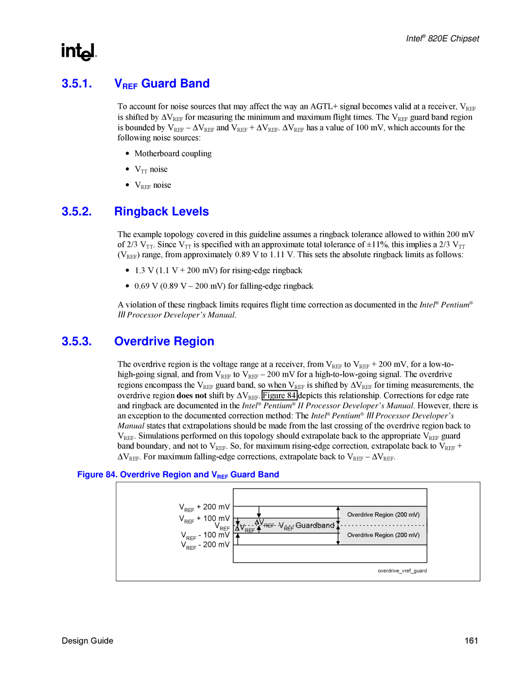
Overdrive Region
Vref Guard Band
Ringback Levels
Flight Time Definition and Measurement
Conclusion
Number Name on CK133 Used for Routed to Frequency Voltage
Clock Generation
Intel 820E Chipset Platform System Clocks
Intel 820E Chipset Platform Clock Distribution
LPCCLK, Pciclk
Intel 820E Chipset Platform Clock Skews
Relationship Skew Pin-to-Pin ps Board ps Total ps Min Max
±TBD3
Intel 820E Chipset Clock Routing Guidelines1,2
CK133/DRCG Pin Name Component
Intel 820E Chipset Platform System Clock Cross-Reference
2. CK133 to Drcg
Component Placement and Interconnection Layout Requirements
1 .318 MHz Crystal to CK133
MCH to Drcg
MCH-to-DRCG Routing Diagram
Trace Length
DRCG-to-RDRAM Channel
Trace Geometry
Clock From Length inches Section
Differential Clock Routing Diagram Sections A, C & D
External Drcg Component Values1,2
Drcg Impedance Matching Circuit
Component Nominal Value
CMID, CMID2
Clock Routing Guidelines for Intel PGA370 Designs
AGP Clock Routing Guidelines
Series Termination Resistors for CK133 Clock Outputs
Drcg Layout Example
Decoupling Recommendation for CK133 and Drcg
Unused Outputs
Unused Output Termination
Buffer Name CC Range Impedance If Unused Output
Drcg Frequency Selection and the DRCG+
Drcg Frequency Selection Table and Jitter Specification
DRCG+ Frequency Selection
DRCG+ Frequency Selection Schematic
PCB Materials
Stack-Up Requirement
Test Coupon Design Guidelines
Design Process
Inner-Layer Routing
Recommended Stack-Up
Stack-Up Examples
Sample SM max Resin %
Field Solver vs. Zcalc
Impedance Calculation Tools
Board Impedance/Stack-up Summary
Testing Board Impedance
182 Design Guide
Term Definition
Power Delivery
Terminology and Definitions
Intel 820E Chipset Power Delivery Example
VCC
Dual Switch
Vbsy
3VSB
V and 2.5 V Power Sequencing Schottky Diode
VSB
ICH2 1.8 V / 3.3 V Power Sequencing
4 .3V/V5REF Sequencing
Example 1.8V/3.3V Power Sequencing Circuit
Vref
Excessive Power Consumption by 64/72-Mbit Rdram
Option 1 Reduce the Clock Frequency During Initialization
Use a GPO to Reduce Drcg Frequency
Example of ICH2 Power Plane Split
ICH2 Power Plane Split
Features
Thermal Design Power
Intel 820E Chipset Component Thermal Design Power
Component Thermal Design Power 133/400 MHz
Vendor Intel Contact Contact Information
Glue Chip Vendors
Reference Design Feature Set
Appendix a Reference Design Schematics Uniprocessor
196 Design Guide
Drawn by PCG Platform Design Project PCG AE
REV
Prairie City Road
FOLSOM, California Last Revised Sheet
Device Table
Block Diagram
AH8
AK8
AN9
AL9
VCMOS15
CPURST#R2 DBRESET#
Gtlref
Tckr TDI Tmsr
Clock Synthesizer
Ramref
Hubref Ramrefr
Connagpref
Hubref Agpref Ramrefb Ramrefa Gtlrefb Gtlrefa Host
GAD0 GAD1
GAD0
GAD1 GAD2
GAD2 GAD3
AD1
AD0
AD2
AD3
CR4
ACRESET#
Vbatcr 1UF
Rtcrstjp
Fwhic Vcca LFRAME#/FWH4 NC3 NC4 INIT# HINIT# NC5 RFU36
NC1 Gnda
NC6 RFU35 FGPI4 RFU34 NC8 RFU33 Fwhpclk CLK RFU32
VCC10 VCC31 Vppr VPP GND30 PCIRST# GND29
RSRV4/RESET SWP
SWP RSRV4/RESET
TERMDQA80
Rimm LDQA0
Super I/O
AC’97 Audio
Micin
Micinr Micinfb
Micinc
DB15AUDSTK
Communication And Network Riser CNR
ACSDATAIN0ICH2 ACSYNCICH2 ACSDATAOUTICH2
Stubs on AC97 Link
RP7
ACSDATAIN0CNR Acsynccnr Acsdataoutcnr
LAN 82562EH
82562ET/EM
LAN RJ11 For 82562EH
Lanactled
LAN RJ45 For 82562ET/EM
H1138ARAGONITE
Y5 Xtal Y2 Xtal LANCLKX1
25MHZ
R381LANCLKX2
LAN Option Intel PART#
Stuff for 82562EH
Power LED
Power SW
SW1
VCC12 Irtx
TYPEDET#
AGP4XU20 AGPOC#
USBAGP+ B4 Usbagp
Agpclkconn B7 CLK
PCI3CON PTRST# Ptck
VCC5 VCC12
Ptms
Ptdi
PCI Connectors
IDE Connectors
USB Connectors
Port Parallel
Serial Ports
Keyboard/Mouse/Floppy
VCC5 JOY1XR JOY2XR Midioutr JOY2YR JOY1YR Midiinr
Game Port
FAULT# IFB
VRM Fault VRM IFB
Vccvid REV Project
Imax VRM G1 VRM G2
Voltage Regulators
VCC33SBYTG VCC33SBYSW VCC25SBY
1UF-X7R
VCC5DUAL VCC33SBY VCC33SBYCOSC VCC33SBYRUN VCC33SBYITH
SBY ITH R
Power Connector
HREQ#0
BPRI# DBSY#
PCI/AGP Pullups/Pulldowns
Termcmd Termsck
Rambus* Termination
Decoupling
Bulk Decoupling Drawn by PCG Platform Design Project PCG AE
VCMOS18SBY
Revision History Drawn by PCG Platform Design Project PCG AE
Revision History
Probe Connector
Hub Interface Connector For debug only
TESTCLK66 HL0 HL1 HL2 HL3 HL9 Hlstb HLSTB#
HL8 HL4 HL5 HL6 HL7