DS33Z41 Quad IMUX Ethernet Mapper
7 PIN DESCRIPTIONS
7.1Pin Functional Description
Note that all digital pins are inout pins in JTAG mode. This feature increases the effectiveness of board level ATPG patterns.
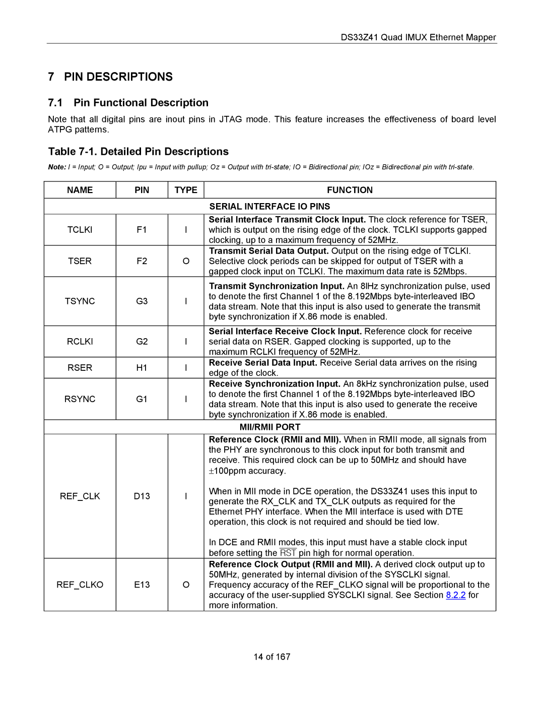
Table 7-1. Detailed Pin Descriptions
Note: I = Input; O = Output; Ipu = Input with pullup; Oz = Output with
NAME | PIN | TYPE | FUNCTION | |
|
|
|
| |
|
|
| SERIAL INTERFACE IO PINS | |
|
|
|
| |
|
|
| Serial Interface Transmit Clock Input. The clock reference for TSER, | |
TCLKI | F1 | I | which is output on the rising edge of the clock. TCLKI supports gapped | |
|
|
| clocking, up to a maximum frequency of 52MHz. | |
TSER | F2 | O | Transmit Serial Data Output. Output on the rising edge of TCLKI. | |
Selective clock periods can be skipped for output of TSER with a | ||||
|
|
| gapped clock input on TCLKI. The maximum data rate is 52Mbps. | |
|
|
| Transmit Synchronization Input. An 8lHz synchronization pulse, used | |
TSYNC | G3 | I | to denote the first Channel 1 of the 8.192Mbps | |
data stream. Note that this input is also used to generate the transmit | ||||
|
|
| ||
|
|
| byte synchronization if X.86 mode is enabled. | |
|
|
|
| |
RCLKI | G2 | I | Serial Interface Receive Clock Input. Reference clock for receive | |
serial data on RSER. Gapped clocking is supported, up to the | ||||
|
|
| maximum RCLKI frequency of 52MHz. | |
RSER | H1 | I | Receive Serial Data Input. Receive Serial data arrives on the rising | |
edge of the clock. | ||||
|
|
| ||
|
|
| Receive Synchronization Input. An 8kHz synchronization pulse, used | |
RSYNC | G1 | I | to denote the first Channel 1 of the 8.192Mbps | |
data stream. Note that this input is also used to generate the receive | ||||
|
|
| ||
|
|
| byte synchronization if X.86 mode is enabled. | |
|
|
| MII/RMII PORT | |
|
|
| Reference Clock (RMII and MII). When in RMII mode, all signals from | |
|
|
| the PHY are synchronous to this clock input for both transmit and | |
|
|
| receive. This required clock can be up to 50MHz and should have | |
|
|
| ±100ppm accuracy. | |
REF_CLK | D13 | I | When in MII mode in DCE operation, the DS33Z41 uses this input to | |
generate the RX_CLK and TX_CLK outputs as required for the | ||||
|
|
| ||
|
|
| Ethernet PHY interface. When the MII interface is used with DTE | |
|
|
| operation, this clock is not required and should be tied low. | |
|
|
| In DCE and RMII modes, this input must have a stable clock input | |
|
|
| before setting the RST pin high for normal operation. | |
|
|
| Reference Clock Output (RMII and MII). A derived clock output up to | |
REF_CLKO | E13 | O | 50MHz, generated by internal division of the SYSCLKI signal. | |
Frequency accuracy of the REF_CLKO signal will be proportional to the | ||||
|
|
| accuracy of the | |
|
|
| more information. |
14 of 167