DS33Z41 Quad IMUX Ethernet Mapper
8.7Device Interrupts
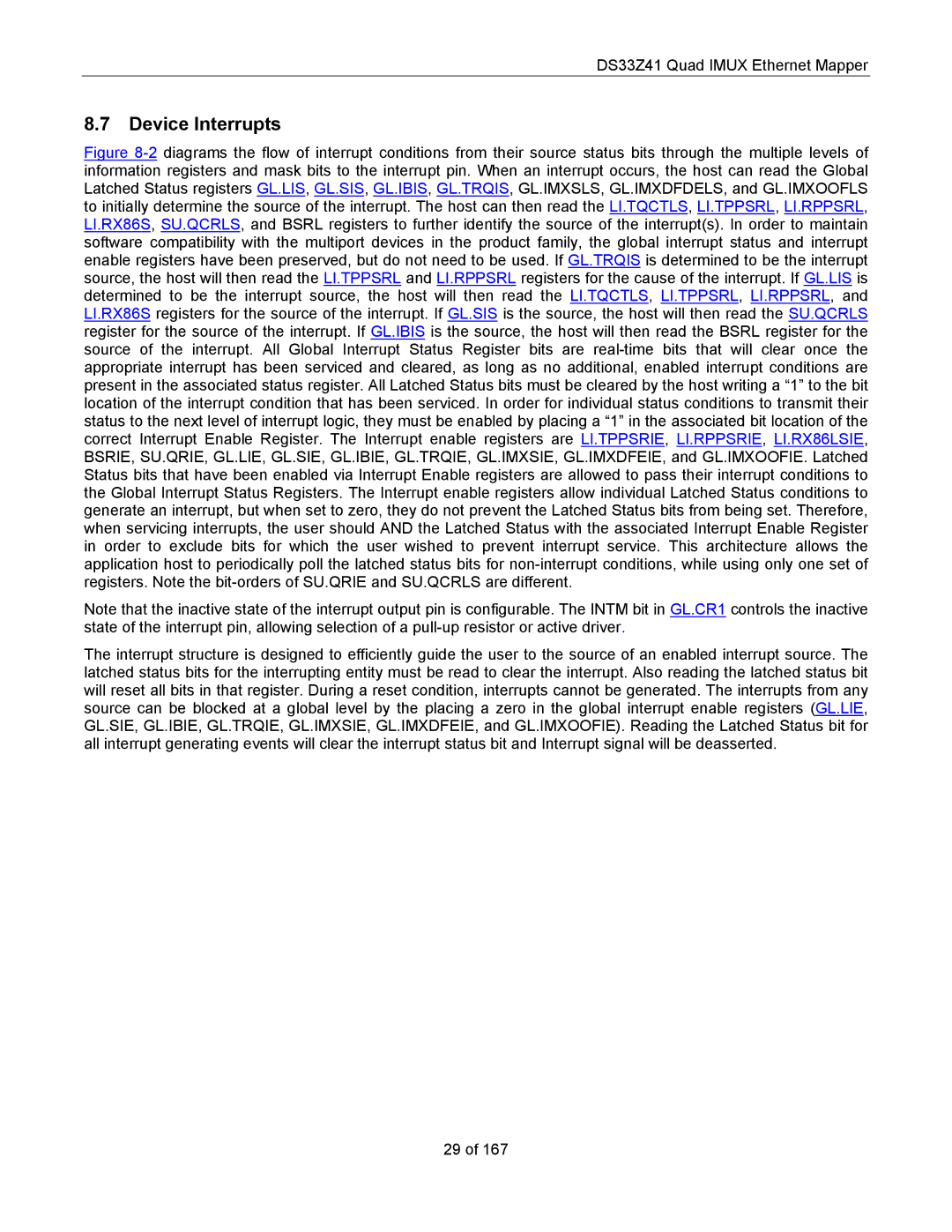
Figure 8-2 diagrams the flow of interrupt conditions from their source status bits through the multiple levels of information registers and mask bits to the interrupt pin. When an interrupt occurs, the host can read the Global Latched Status registers GL.LIS, GL.SIS, GL.IBIS, GL.TRQIS, GL.IMXSLS, GL.IMXDFDELS, and GL.IMXOOFLS to initially determine the source of the interrupt. The host can then read the LI.TQCTLS, LI.TPPSRL, LI.RPPSRL, LI.RX86S, SU.QCRLS, and BSRL registers to further identify the source of the interrupt(s). In order to maintain software compatibility with the multiport devices in the product family, the global interrupt status and interrupt enable registers have been preserved, but do not need to be used. If GL.TRQIS is determined to be the interrupt source, the host will then read the LI.TPPSRL and LI.RPPSRL registers for the cause of the interrupt. If GL.LIS is determined to be the interrupt source, the host will then read the LI.TQCTLS, LI.TPPSRL, LI.RPPSRL, and LI.RX86S registers for the source of the interrupt. If GL.SIS is the source, the host will then read the SU.QCRLS register for the source of the interrupt. If GL.IBIS is the source, the host will then read the BSRL register for the source of the interrupt. All Global Interrupt Status Register bits are real-time bits that will clear once the appropriate interrupt has been serviced and cleared, as long as no additional, enabled interrupt conditions are present in the associated status register. All Latched Status bits must be cleared by the host writing a “1” to the bit location of the interrupt condition that has been serviced. In order for individual status conditions to transmit their status to the next level of interrupt logic, they must be enabled by placing a “1” in the associated bit location of the correct Interrupt Enable Register. The Interrupt enable registers are LI.TPPSRIE, LI.RPPSRIE, LI.RX86LSIE, BSRIE, SU.QRIE, GL.LIE, GL.SIE, GL.IBIE, GL.TRQIE, GL.IMXSIE, GL.IMXDFEIE, and GL.IMXOOFIE. Latched Status bits that have been enabled via Interrupt Enable registers are allowed to pass their interrupt conditions to the Global Interrupt Status Registers. The Interrupt enable registers allow individual Latched Status conditions to generate an interrupt, but when set to zero, they do not prevent the Latched Status bits from being set. Therefore, when servicing interrupts, the user should AND the Latched Status with the associated Interrupt Enable Register in order to exclude bits for which the user wished to prevent interrupt service. This architecture allows the application host to periodically poll the latched status bits for non-interrupt conditions, while using only one set of registers. Note the bit-orders of SU.QRIE and SU.QCRLS are different.
Note that the inactive state of the interrupt output pin is configurable. The INTM bit in GL.CR1 controls the inactive state of the interrupt pin, allowing selection of a
The interrupt structure is designed to efficiently guide the user to the source of an enabled interrupt source. The latched status bits for the interrupting entity must be read to clear the interrupt. Also reading the latched status bit will reset all bits in that register. During a reset condition, interrupts cannot be generated. The interrupts from any source can be blocked at a global level by the placing a zero in the global interrupt enable registers (GL.LIE, GL.SIE, GL.IBIE, GL.TRQIE, GL.IMXSIE, GL.IMXDFEIE, and GL.IMXOOFIE). Reading the Latched Status bit for all interrupt generating events will clear the interrupt status bit and Interrupt signal will be deasserted.
29 of 167