|
|
|
| DS33Z41 Quad IMUX Ethernet Mapper |
|
|
|
|
|
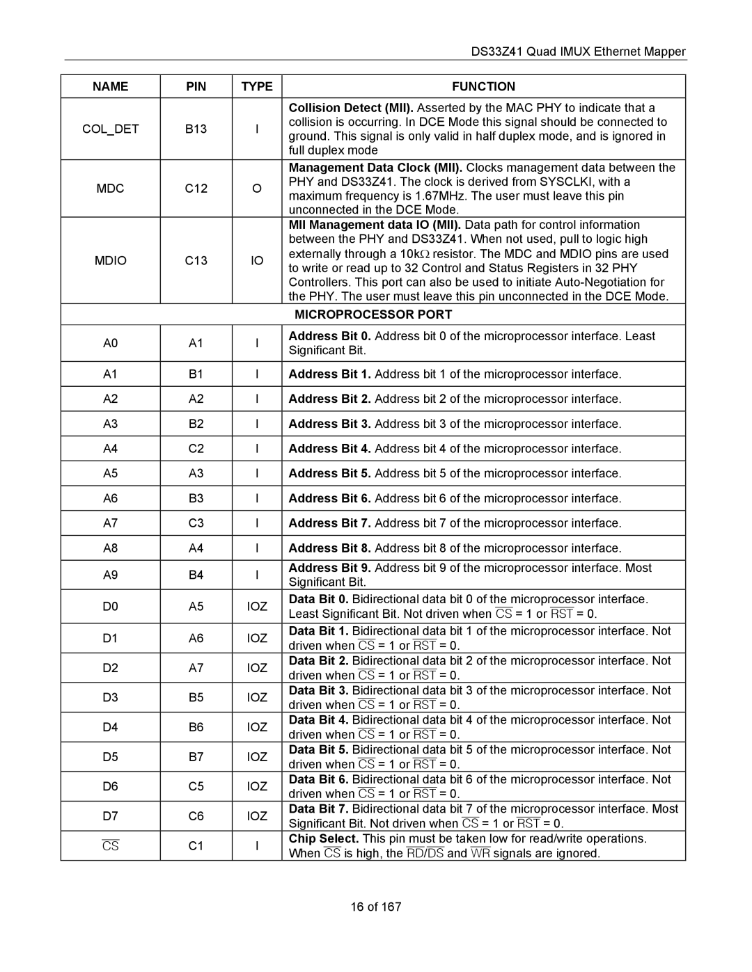
| NAME | PIN | TYPE | FUNCTION |
|
|
|
|
|
|
|
|
| Collision Detect (MII). Asserted by the MAC PHY to indicate that a |
| COL_DET | B13 | I | collision is occurring. In DCE Mode this signal should be connected to |
| ground. This signal is only valid in half duplex mode, and is ignored in | |||
|
|
|
| |
|
|
|
| full duplex mode |
|
|
|
| Management Data Clock (MII). Clocks management data between the |
| MDC | C12 | O | PHY and DS33Z41. The clock is derived from SYSCLKI, with a |
| maximum frequency is 1.67MHz. The user must leave this pin | |||
|
|
|
| |
|
|
|
| unconnected in the DCE Mode. |
|
|
|
| MII Management data IO (MII). Data path for control information |
|
|
|
| between the PHY and DS33Z41. When not used, pull to logic high |
| MDIO | C13 | IO | externally through a 10kΩ resistor. The MDC and MDIO pins are used |
| to write or read up to 32 Control and Status Registers in 32 PHY | |||
|
|
|
| |
|
|
|
| Controllers. This port can also be used to initiate |
|
|
|
| the PHY. The user must leave this pin unconnected in the DCE Mode. |
|
|
|
| MICROPROCESSOR PORT |
|
|
|
|
|
| A0 | A1 | I | Address Bit 0. Address bit 0 of the microprocessor interface. Least |
| Significant Bit. | |||
|
|
|
| |
| A1 | B1 | I | Address Bit 1. Address bit 1 of the microprocessor interface. |
|
|
|
|
|
| A2 | A2 | I | Address Bit 2. Address bit 2 of the microprocessor interface. |
|
|
|
|
|
| A3 | B2 | I | Address Bit 3. Address bit 3 of the microprocessor interface. |
|
|
|
|
|
| A4 | C2 | I | Address Bit 4. Address bit 4 of the microprocessor interface. |
|
|
|
|
|
| A5 | A3 | I | Address Bit 5. Address bit 5 of the microprocessor interface. |
|
|
|
|
|
| A6 | B3 | I | Address Bit 6. Address bit 6 of the microprocessor interface. |
|
|
|
|
|
| A7 | C3 | I | Address Bit 7. Address bit 7 of the microprocessor interface. |
|
|
|
|
|
| A8 | A4 | I | Address Bit 8. Address bit 8 of the microprocessor interface. |
|
|
|
|
|
| A9 | B4 | I | Address Bit 9. Address bit 9 of the microprocessor interface. Most |
| Significant Bit. | |||
|
|
|
| |
| D0 | A5 | IOZ | Data Bit 0. Bidirectional data bit 0 of the microprocessor interface. |
| Least Significant Bit. Not driven when CS = 1 or RST = 0. | |||
|
|
|
| |
| D1 | A6 | IOZ | Data Bit 1. Bidirectional data bit 1 of the microprocessor interface. Not |
| driven when CS = 1 or RST = 0. | |||
|
|
|
| |
| D2 | A7 | IOZ | Data Bit 2. Bidirectional data bit 2 of the microprocessor interface. Not |
| driven when CS = 1 or RST = 0. | |||
|
|
|
| |
| D3 | B5 | IOZ | Data Bit 3. Bidirectional data bit 3 of the microprocessor interface. Not |
| driven when CS = 1 or RST = 0. | |||
|
|
|
| |
| D4 | B6 | IOZ | Data Bit 4. Bidirectional data bit 4 of the microprocessor interface. Not |
| driven when CS = 1 or RST = 0. | |||
|
|
|
| |
| D5 | B7 | IOZ | Data Bit 5. Bidirectional data bit 5 of the microprocessor interface. Not |
| driven when CS = 1 or RST = 0. | |||
|
|
|
| |
| D6 | C5 | IOZ | Data Bit 6. Bidirectional data bit 6 of the microprocessor interface. Not |
| driven when CS = 1 or RST = 0. | |||
|
|
|
| |
| D7 | C6 | IOZ | Data Bit 7. Bidirectional data bit 7 of the microprocessor interface. Most |
| Significant Bit. Not driven when CS = 1 or RST = 0. | |||
|
|
|
| |
| CS | C1 | I | Chip Select. This pin must be taken low for read/write operations. |
| When CS is high, the RD/DS and WR signals are ignored. | |||
|
|
|
| |
|
|
|
| 16 of 167 |
Page 16
Image 16