DS33Z41 Quad IMUX Ethernet Mapper
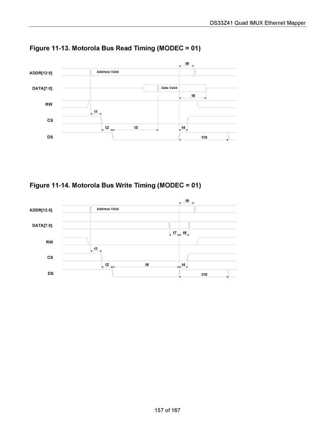
Figure 11-13. Motorola Bus Read Timing (MODEC = 01)
|
|
| t9 |
ADDR[12:0] | Address Valid |
|
|
DATA[7:0] |
|
| Data Valid |
|
|
| t5 |
RW |
|
|
|
| t1 |
|
|
CS |
|
|
|
| t2 | t3 | t4 |
DS |
|
| t10 |
Figure 11-14. Motorola Bus Write Timing (MODEC = 01)
ADDR[12:0] | Address Valid |
DATA[7:0]
RW
t1
CS
t2t6
DS
t9
t7 t8
t4
t10
157 of 167