|
|
|
| DS33Z41 Quad IMUX Ethernet Mapper |
|
|
|
|
|
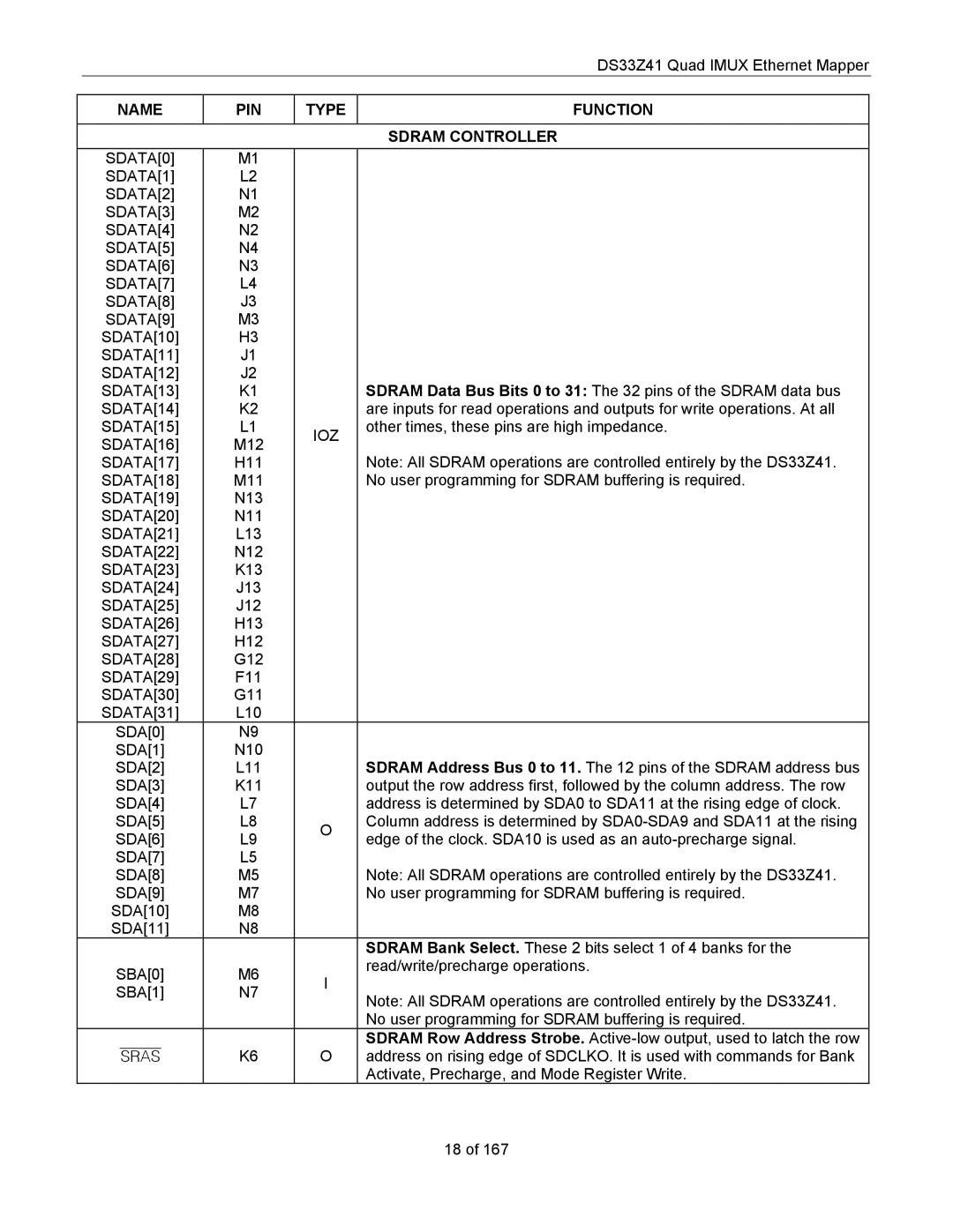
| NAME | PIN | TYPE | FUNCTION |
|
|
|
|
|
|
|
|
| SDRAM CONTROLLER |
| SDATA[0] | M1 |
|
|
| SDATA[1] | L2 |
|
|
| SDATA[2] | N1 |
|
|
| SDATA[3] | M2 |
|
|
| SDATA[4] | N2 |
|
|
| SDATA[5] | N4 |
|
|
| SDATA[6] | N3 |
|
|
| SDATA[7] | L4 |
|
|
| SDATA[8] | J3 |
|
|
| SDATA[9] | M3 |
|
|
| SDATA[10] | H3 |
|
|
| SDATA[11] | J1 |
|
|
| SDATA[12] | J2 |
| SDRAM Data Bus Bits 0 to 31: The 32 pins of the SDRAM data bus |
| SDATA[13] | K1 |
| |
| SDATA[14] | K2 |
| are inputs for read operations and outputs for write operations. At all |
| SDATA[15] | L1 | IOZ | other times, these pins are high impedance. |
| SDATA[16] | M12 |
| |
|
| Note: All SDRAM operations are controlled entirely by the DS33Z41. | ||
| SDATA[17] | H11 |
| |
| SDATA[18] | M11 |
| No user programming for SDRAM buffering is required. |
| SDATA[19] | N13 |
|
|
| SDATA[20] | N11 |
|
|
| SDATA[21] | L13 |
|
|
| SDATA[22] | N12 |
|
|
| SDATA[23] | K13 |
|
|
| SDATA[24] | J13 |
|
|
| SDATA[25] | J12 |
|
|
| SDATA[26] | H13 |
|
|
| SDATA[27] | H12 |
|
|
| SDATA[28] | G12 |
|
|
| SDATA[29] | F11 |
|
|
| SDATA[30] | G11 |
|
|
| SDATA[31] | L10 |
|
|
| SDA[0] | N9 |
|
|
| SDA[1] | N10 |
| SDRAM Address Bus 0 to 11. The 12 pins of the SDRAM address bus |
| SDA[2] | L11 |
| |
| SDA[3] | K11 |
| output the row address first, followed by the column address. The row |
| SDA[4] | L7 |
| address is determined by SDA0 to SDA11 at the rising edge of clock. |
| SDA[5] | L8 | O | Column address is determined by |
| SDA[6] | L9 | edge of the clock. SDA10 is used as an | |
|
| |||
| SDA[7] | L5 |
| Note: All SDRAM operations are controlled entirely by the DS33Z41. |
| SDA[8] | M5 |
| |
| SDA[9] | M7 |
| No user programming for SDRAM buffering is required. |
| SDA[10] | M8 |
|
|
| SDA[11] | N8 |
|
|
|
|
|
| SDRAM Bank Select. These 2 bits select 1 of 4 banks for the |
| SBA[0] | M6 | I | read/write/precharge operations. |
|
| |||
| SBA[1] | N7 | Note: All SDRAM operations are controlled entirely by the DS33Z41. | |
|
| |||
|
|
|
| |
|
|
|
| No user programming for SDRAM buffering is required. |
|
| K6 | O | SDRAM Row Address Strobe. |
| SRAS | address on rising edge of SDCLKO. It is used with commands for Bank | ||
|
|
|
| Activate, Precharge, and Mode Register Write. |
|
|
|
| 18 of 167 |
Page 18
Image 18