|
|
| DS33Z41 Quad IMUX Ethernet Mapper | |
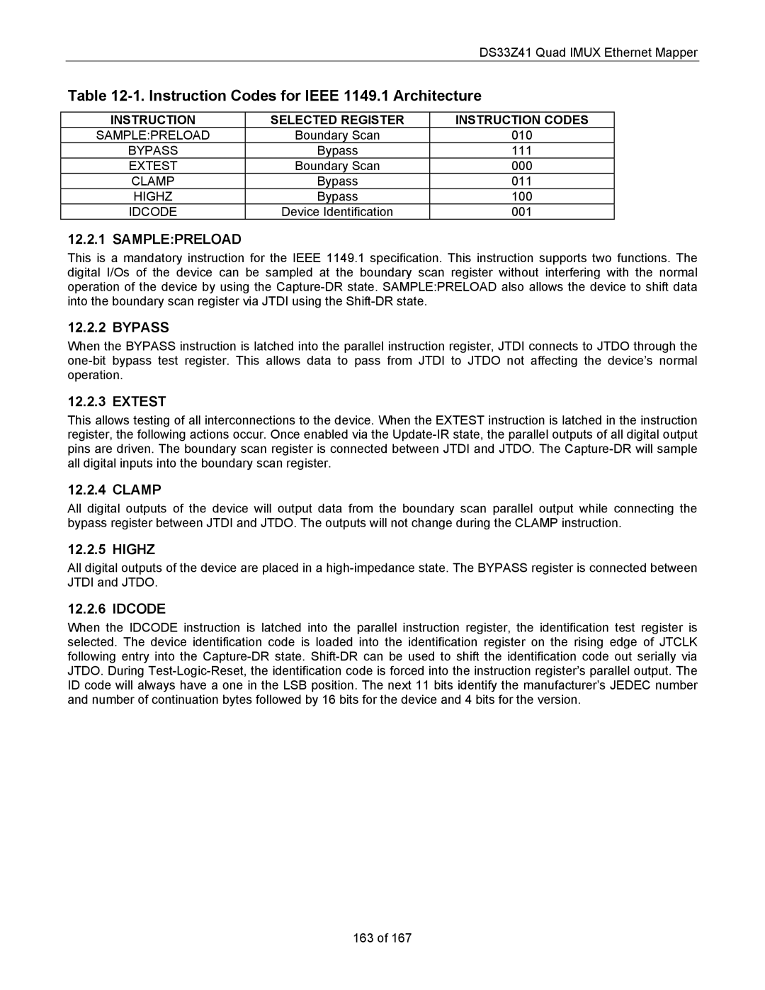
| Table | |||
|
|
|
| |
| INSTRUCTION | SELECTED REGISTER | INSTRUCTION CODES |
|
| SAMPLE:PRELOAD | Boundary Scan | 010 |
|
| BYPASS | Bypass | 111 |
|
| EXTEST | Boundary Scan | 000 |
|
| CLAMP | Bypass | 011 |
|
| HIGHZ | Bypass | 100 |
|
| IDCODE | Device Identification | 001 |
|
12.2.1 SAMPLE:PRELOAD
This is a mandatory instruction for the IEEE 1149.1 specification. This instruction supports two functions. The digital I/Os of the device can be sampled at the boundary scan register without interfering with the normal operation of the device by using the
12.2.2 BYPASS
When the BYPASS instruction is latched into the parallel instruction register, JTDI connects to JTDO through the
12.2.3 EXTEST
This allows testing of all interconnections to the device. When the EXTEST instruction is latched in the instruction register, the following actions occur. Once enabled via the
12.2.4 CLAMP
All digital outputs of the device will output data from the boundary scan parallel output while connecting the bypass register between JTDI and JTDO. The outputs will not change during the CLAMP instruction.
12.2.5 HIGHZ
All digital outputs of the device are placed in a
12.2.6 IDCODE
When the IDCODE instruction is latched into the parallel instruction register, the identification test register is selected. The device identification code is loaded into the identification register on the rising edge of JTCLK following entry into the
163 of 167