DS33Z41 Quad IMUX Ethernet Mapper
Bit 0: BIST
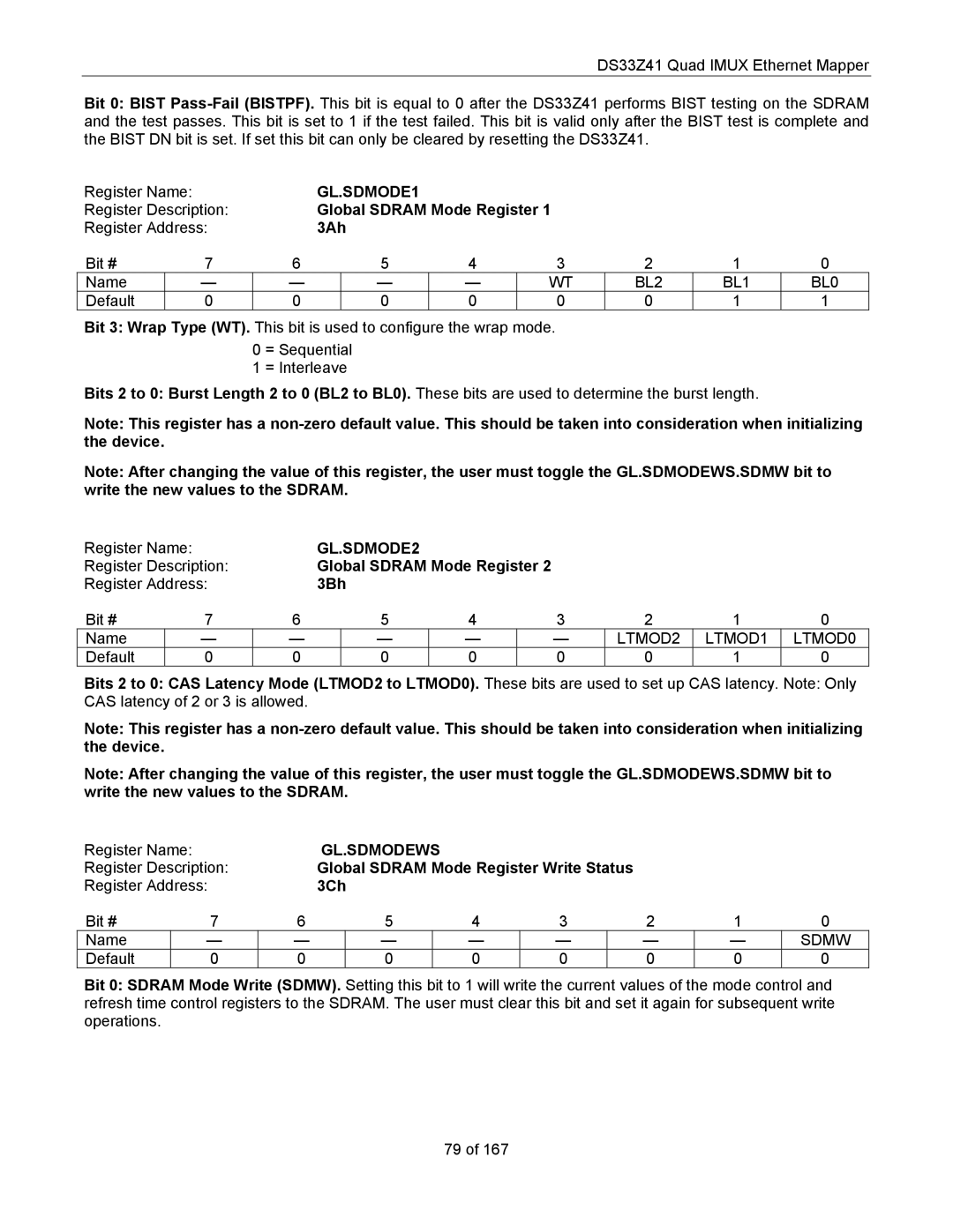
Register Name: |
|
| GL.SDMODE1 |
|
|
|
|
| ||
Register Description: |
| Global SDRAM Mode Register 1 |
|
|
| |||||
Register Address: |
| 3Ah |
|
|
|
|
| |||
Bit # | 7 | 6 | 5 | 4 | 3 | 2 | 1 | 0 | ||
Name |
| — | — |
| — | — | WT | BL2 | BL1 | BL0 |
Default |
| 0 | 0 |
| 0 | 0 | 0 | 0 | 1 | 1 |
Bit 3: Wrap Type (WT). This bit is used to configure the wrap mode.
0 = Sequential
1 = Interleave
Bits 2 to 0: Burst Length 2 to 0 (BL2 to BL0). These bits are used to determine the burst length.
Note: This register has a
Note: After changing the value of this register, the user must toggle the GL.SDMODEWS.SDMW bit to write the new values to the SDRAM.
Register Name: |
|
| GL.SDMODE2 |
|
|
|
|
|
| ||
Register Description: |
| Global SDRAM Mode Register 2 |
|
|
|
| |||||
Register Address: |
| 3Bh |
|
|
|
|
|
| |||
Bit # | 7 | 6 | 5 | 4 |
| 3 | 2 | 1 | 0 | ||
Name |
| — | — |
| — | — |
| — | LTMOD2 | LTMOD1 | LTMOD0 |
Default |
| 0 | 0 |
| 0 | 0 |
| 0 | 0 | 1 | 0 |
Bits 2 to 0: CAS Latency Mode (LTMOD2 to LTMOD0). These bits are used to set up CAS latency. Note: Only CAS latency of 2 or 3 is allowed.
Note: This register has a
Note: After changing the value of this register, the user must toggle the GL.SDMODEWS.SDMW bit to write the new values to the SDRAM.
Register Name: |
|
| GL.SDMODEWS |
|
|
|
|
|
| |||
Register Description: |
| Global SDRAM Mode Register Write Status |
|
|
| |||||||
Register Address: |
| 3Ch |
|
|
|
|
|
| ||||
Bit # | 7 | 6 | 5 |
| 4 | 3 |
| 2 | 1 | 0 | ||
Name |
| — | — |
| — |
| — | — |
| — | — | SDMW |
Default |
| 0 | 0 |
| 0 |
| 0 | 0 |
| 0 | 0 | 0 |
Bit 0: SDRAM Mode Write (SDMW). Setting this bit to 1 will write the current values of the mode control and refresh time control registers to the SDRAM. The user must clear this bit and set it again for subsequent write operations.
79 of 167